Numerical simulations enable deep studies of new laser, detector, and absorber technologies in the spectral range between the microwave and the infrared. with Simulation Software
Andrew Strikwerda, COMSOL
Rather than coining the phrase “x-ray vision,” perhaps comic book writers should have called it “terahertz vision” instead. The precise blend of electromagnetic and material properties in the terahertz spectrum enables efficient applications such as simultaneous noncontact package inspection with spectroscopic characterization — to determine, for example, whether a package contains baking flour or an illegal or otherwise dangerous substance. This can be determined without opening the package and while returning images of the package contents with submillimeter precision.
This use case and many others are possible by using terahertz radiation. However, implementations are not yet commonplace because many of the practical engineering components needed to build them are still being developed. Fortunately, the use of numerical simulation is accelerating the design of components for terahertz-based systems.
The terahertz gap
The terahertz spectrum is a largely untapped spectral range situated between the microwave and the far-infrared. There is no firm consensus on the precise bounds of the terahertz region. Depending on
whom you ask, the range covers from 0.3 to 3 THz, from 0.1 to 10 THz, or it even extends to frequencies as high as 30 THz. Because of the variety of units used in various disciplines, it’s useful to define radiation at 1 THz as equivalent to a wavelength of 300 μm, photon energy of 4.1 meV, a wave number of 33.3 cm−1, or
a temperature of 48 K (Figure 1).
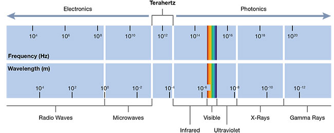
Figure 1. The terahertz spectral range lies between the microwave and the infrared ranges. Behavior in these bounding ranges is largely dominated by the electron and the photon, respectively. In the transition region, a dearth of terahertz radiation sources, detectors, modulators, and other optical components has left a ‘terahertz gap’ that product developers are now finding ways to populate. Courtesy of COMSOL.
Regardless of which units are preferred, the scientific and technological possibilities of the spectrum are exciting and largely untapped. The easily accessible off-the-shelf components required for large-scale adoption — such as terahertz radiation sources, detectors, modulators, and other optical elements — are still being fully developed. These missing fundamental building blocks are often referred to as the “terahertz gap.”
Progress on filling this gap with technological building blocks has been slow but steady, aided most recently by numerical simulation of terahertz systems and components. Electromagnetic simulation, which numerically solves Maxwell’s equations for a given geometry and material properties, yields high-fidelity design analysis, accelerates design optimization, and can drastically reduce the number of fabrication and testing iterations required in product development.
Terahertz waves open new doors
The exciting technological possibilities of the terahertz spectrum revolve around several key properties of terahertz radiation and how materials respond to it. These five properties are:
• Transparency. Many common
materials, such as those used in
packaging, are transparent to
terahertz waves.
• High resolution. Terahertz radiation has a shorter wavelength than millimeter waves, which enhances spatial resolution for imaging applications.
• Reduced scattering. Terahertz waves have a longer wavelength than infrared radiation, which reduces the scattering loss through materials and particulate matter and enables penetrative detection.
• Safety. Terahertz radiation is
generally considered safer than x-rays for humans because its low photon energy is nonionizing.
• Spectral fingerprints. Many chemical and biological materials of interest have unique spectral fingerprints in the terahertz spectrum.
These properties evoke high-profile commercial use cases in imaging, security, nondestructive testing, and quality assurance. In reference to the example of noncontact package inspection, it is clear that the unique combination of material transparency, submillimeter-wave spatial resolution, and spectroscopic analysis could significantly affect customs and goods transport. In the pharmaceutical industry, drugs could be scanned to determine whether the composition is authentic or has been substituted or degraded.
In another use case, a terahertz system could inspect materials such as composites, foams, and ceramics to identify internal voids or cracks that could lead to deterioration or catastrophic failure. Due to the terahertz transparency of these materials, it is possible to obtain accurate depth information while still achieving submillimeter wave resolution. Current nondestructive testing methods in the infrared (IR) spectrum tend to have high spatial resolution but poor depth resolution, whereas radio frequency (RF) methods have the inverse characteristics. The terahertz spectrum is a sweet spot in which both of these resolutions can be simultaneously achieved.
While initial progress has been made in these application spaces in the academic research literature, widespread industry adoption has not occurred yet.
In addition to direct commercial applications, several interesting physical phenomena in the terahertz spectrum could lead to improved understanding and development of complex materials. The terahertz range covers characteristic energies for several physical phenomena — including excitons, phonons, plasmon dynamics, charge transport phenomena, and Cooper pairs — that are responsible for superconductivity (Figure 2).
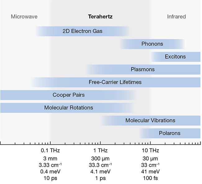
Figure 2. Physical phenomena with interesting characteristics in the terahertz spectrum. Courtesy of COMSOL.
Using the terahertz spectrum and terahertz time-domain spectroscopy (THz-TDS) to study the behavior of these phenomena in materials has led to a greater understanding of their function, with the promise of better materials-science development in the future. For example, THz-TDS systems — as contact-free probes of electrical conductivity — deliver subpicosecond temporal resolution, which is useful to research phase transitions, topological insulators, 2D materials such as graphene, and many more emerging materials.
Challenges in the terahertz spectrum
The transitional or hybrid nature of the terahertz spectrum impedes progress in filling in the terahertz gap and, therefore, in exploiting the region. The microwave and infrared ranges between which the terahertz spectrum exists can be thought of as being characterized by the behaviors of electrons and photons, respectively. Both of these perspectives break down in the terahertz spectrum. Much of the technological progress in this spectral range has come from developing new techniques or blending RF and optical approaches.
The development of commercial terahertz sources and detectors is still in the early stages. Consequently, only a small number of terahertz optical components are commercially available.
Because the electron dominates the millimeter wave or RF spectrum, the high-frequency limit of the range can be thought of as the time it takes for an electron to physically traverse a transistor. This picture is greatly simplified, of course, but it illustrates why substantial progress has been made by reducing the size of transistors and developing high-electron-mobility transistors. While the progress has been steady, it has become clear that fundamentally new approaches are required.
On the other side of the terahertz gap are the infrared and optical spectra, which are dominated by the photon. From a conceptual standpoint, the lower boundary of the IR spectrum can be thought of as the amount of photon energy it takes to excite a semiconductor bandgap, a process ultimately limited by the operating temperature of the device. For reference, the photon energy associated with a room temperature of 20 ºC is 25 meV, whereas the photon energy at 1 THz is 4.1 meV, which corresponds to a temperature of
48 K. As a result, terahertz bandgaps will be thermally populated at room temperature, rendering them unusable without
additional cooling. This severely limits the use of many traditional optical components, such as photodiodes and quantum cascade lasers.
Terahertz technology progress
Despite these challenges, a reasonable amount of progress has been made over the last decade in commercializing terahertz sources and detectors, largely driven by the miniaturization and increased resiliency of commercial laser systems.
Although tabletop terahertz spectroscopy systems have existed in research laboratories for more than 30 years, the systems are quite sensitive to their environment because they rely on ultrashort optical pulses from femtosecond laser systems. The ultrafast pulses are combined with either photoconductive antennas or nonlinear optical processes to generate and detect terahertz waves. Because these ultrafast laser systems have historically required controlled environments and regular tuning to perform adequately, the systems have been unsuitable for widespread industrial application.
Just over a decade ago, however, advancements in stable turnkey systems helped lead to the first commercially available terahertz spectroscopy systems. Commercially available time-domain systems typically rely on ultrafast lasers and fiber-coupled photoconductive antennas, whereas frequency-domain systems replace the ultrafast laser with two continuous-wave lasers that are tuned so that their beat frequency is in the terahertz spectrum. Other methods for passive detection, such as bolometers and pyroelectric detectors, are much less common in terahertz systems.
The development of commercial terahertz sources and detectors is still in the early stages. Consequently, only a small number of terahertz optical components are commercially available. Off-the-shelf lenses and beamsplitters have somewhat filled in this gap, but they are quite bulky, which substantially increases the size of a terahertz system and could limit adoption. More exotic passive components such as low-profile perfect absorbers or spectral filters generally exist only in research laboratories, and active components that can modulate the phase, amplitude, direction, or polarization of the beam are even more rare and are more likely to be found in academic publications than in commercial offerings.
Research and development of novel terahertz components rely on electromagnetic simulation software to design custom-made devices. The maturity and widespread availability of numerical simulation software have improved predictability and accessibility for terahertz component design. Multiphysics simulation can easily create sophisticated designs that combine metamaterial technology with phase-change materials, such as thermally controlled vanadium dioxide (VO2). This accessibility should enable increased availability of off-the-shelf and custom terahertz optics components over the next decade.
Optimizing terahertz absorbers
Virtual prototyping of a perfect terahertz absorber illustrates how simulation advances the development of terahertz
components. Terahertz absorbers can provide spatial and spectral filtering or enhance certain types of terahertz detectors. Detector enhancement is important because most materials have a relatively weak electromagnetic response in the terahertz regime, whereas specially designed metamaterials can reach perfect absorption in a subwavelength thick film.
Through numerical simulation, researchers have optimized absorber designs to achieve perfect absorption at specific frequencies, high absorption over large bandwidths, and polarization sensitivity or insensitivity. These features, combined with the subwavelength footprint of the metamaterial unit cells, can enable high-resolution pixel arrays or detectors optimized for specific chemical signatures.
As a specific example of this, Figure 3 shows the first experimental demonstration of near-unity absorption at terahertz frequencies1,2. Figure 4 shows the corresponding computed absorption spectrum. The structure is a gold, electric split-ring resonator — or an electric-LC (ELC) resonator — on an 8-μm-thick polyimide substrate, which, in turn, is situated on a gold ground plane. Several theories explain the general phenomenon of perfect absorption in metamaterials in various terms, such as deconstructive interference between the ground plane and the ELC layer, but they are not predictive. Numerical analysis is required to assess each specific absorber design and optimize it for a prescribed behavior, such as multiband or angle-sensitive operation.
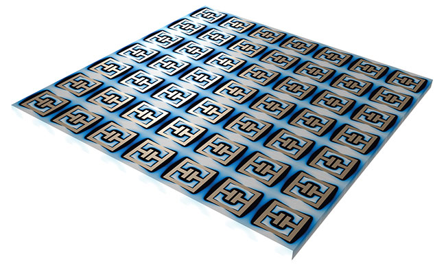
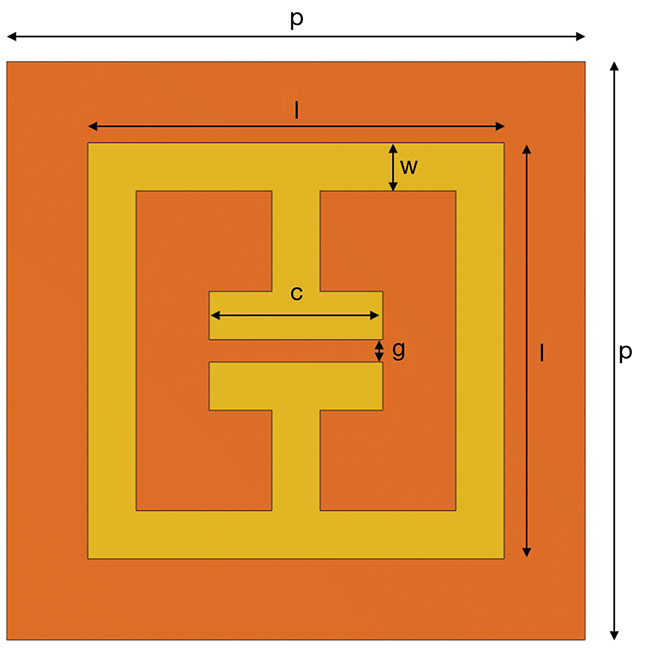
Figure 3. The simulation results for a terahertz absorber structure (top) show the magnitude of the electric field. The unit cell of the absorber (bottom) has a 200-nm layer of gold on an 8-μm polyimide substrate. The polyimide is backed by a continuous ground plane of gold (not shown). Cell dimensions: p = 36 μm, l = 25.9 μm, w = 3 μm, c = 10.8 μm, and g = 1.4 μm. See Reference 2. Courtesy of COMSOL.
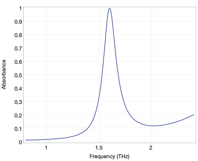
Figure 4. The computed absorption spectrum of the terahertz absorber from Figure 3, with an absorption peak of unity at 1.6 THz. The location of the peak can be moved by adjusting the unit cell geometry. Other geometric changes can add features such as multiband or broadband absorption and polarization dependence. Because of the optically thick ground plane, the transmittance is zero and the reflectance spectrum is R = 1 − A, where A is the absorbance in the figure.
Courtesy of COMSOL.
Simulation also enables design analysis beyond what experiments can deliver. In the example of the absorber, the simulation process solves the loss through the polyimide and gold regions so that the regions of greatest (and least) absorption are well known. Integrating those quantities reveals that approximately 2% of the loss occurs in the ground plane, 48% in the ELC, and the remaining 50% in the polyimide substrate.
Absorption as a function of location is useful for applications in charge separation and transport, nonlinear behavior based on near-field enhancement, or multiphysics simulation. For example, if the application needs to attach the absorber to a terahertz detector instead of a ground plane, the loss information from this simulation can be combined with a heat transfer simulation to create a fully coupled multiphysics simulation to better understand system-level performance.
In conclusion, the terahertz region is an exciting but underused portion of the electromagnetic spectrum. Technological developments such as high-fidelity numerical simulation and robust laser sources are unlocking the possibilities of this spectral range.
Meet the author
Andrew Strikwerda, Ph.D., is a lead applications engineer at COMSOL who specializes in electromagnetics. He has contributed to more than 50 publications, largely in the terahertz spectrum. Strikwerda has a doctorate in
physics from Boston University.
References
1. COMSOL. Simulating metamaterials in
the terahertz regime with COMSOL Multiphysics, www.comsol.com/video/simulating-metamaterials-in-the-terahertz-regime-with-comsol-multiphysics.
2. H. Tao et al. (2008). Highly flexible wide angle of incidence terahertz metamaterial absorber: design, fabrication, and characterization. Phys Rev B, Vol. 78, p. 241103(R).