A Fast, Simple, Accurate Tool
Dr. Iris Bloomer and Dr. Rebecca Mirsky
Broadband spectrophotometers coupled with relatively simple algorithms can provide fast, nondestructive
and comprehensive characterization of thin films.
Designing devices that incorporate ultrathin films is an important means of enhancing yields.
However, characterizing ultrathin films can be extremely challenging for mainstream
metrology tools such as ellipsometers, interferometers and profilometers. One promising
innovation is broadband spectrophotometry: If applied in conjunction with an appropriate
physical model for data analysis, it can provide important information about thin-film
thicknesses and optical properties in a single, nondestructive step.
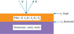
Figure 1. The complexity of thin-film characterization is apparent even when measuring the broadband reflectance
spectrum of a single film deposited on an opaque substrate. Reflectance (R)
is defined as the ratio of the reflected intensity over the incident intensity of
light. The measured reflectance spectrum, R(λ), will depend on values for
the thickness (d), index of refraction (n), extinction coefficient
(k) and energy bandgap (Eg) of the film. It also depends on
the n(λ) and k(λ) values of the substrate, the interface roughness — σ1
(top) and σ2 (bottom) — and the angle of incidence (Θ).
Optical characterization of thin films involves
the determination of film thickness (d), index of refraction (n) and
extinction coefficient (k). The latter two parameters are frequently referred
to as optical constants, but the word “constant” is misleading because
the values of n and k actually depend on the wavelength used to make
the measurement. That is, the n and k values associated with any particular
material may be different at different wavelengths. This is expressed by writing
n = n(λ) and k = k(λ). Another useful parameter is the
film’s energy bandgap (Eg), which represents the minimum photon
energy needed for a direct electronic transition from valance to conduction band.
Broadband spectrophotometry works by
obtaining reflectance and/ or transmittance data over a wide wavelength range. Combined
with a valid physical model, the collected data can provide an analysis of a material’s
thickness, refractive index, extinction coefficient and energy bandgap.
Appropriate physical model
The physical model is necessary because, in general,
spectra for the refractive index and extinction coefficient of any material cannot
be measured directly, but must be deduced from optical measurements such as reflectance,
transmittance or the phase shift of polarized light. This applies also to a film’s
thickness, energy bandgap and interface roughness (σ).
The first step in characterizing any
thin film is to formulate a theoretical algorithm for reflectance in terms of the
n(λ) and k(λ) values for the film and substrate, the film’s
thickness and energy bandgap, and the interface roughness. Although standard Fresnel
coefficients address reflectance of multilayer films in terms of the n, k
and d values of the film and substrate, they do not address n and
k as a function of the wavelength of light. That is, as n(λ) or k(λ).
Incorporating into the Fresnel equations
a physically valid description of refractive index and extinction coefficient as
a function of wavelength as well as a valid description of interface roughness renders
an algorithm for thin-film characterization.
The Forouhi-Bloomer dispersion equations
for refractive index and extinction coefficient constitute a physical model that
is applicable to a wide range of semiconductor and dielectric materials.1,2 The model is valid for measurements ranging
from 190 to 1000 nm, and it is far simpler than other models used to describe these
parameters. All the data reported in this article were obtained using a broadband
spectrophotometric method with the Forouhi-Bloomer dispersion equations.
For example, the n and k
spectra obtained with a spectroscopic ellipsometer can vary widely from sample to
sample and are restricted to a much narrower wavelength range (300 to 610 nm). Also,
mainstream tools such as ellipsometers often employ a table of fixed n and
k values when setting up a model to determine thickness, even though variations
naturally occur during the manufacturing process. In fact, any process change, no
matter how minute, can drastically affect the measurement results.
Understandably, these variations can
have far-reaching implications in the manufacturing environment. Applying a table
of fixed n and k values is especially problematic for ultrathin films
and other tightly toleranced applications involving films of regular thickness.
Establishing a robust physical model is further complicated when the interface between
the layers of film or the substrate surface is rough.
Applications
Traditionally, the characterization of shallow
trench systems has relied on time-consuming and highly localized techniques such
as atomic force microscopy (AFM) or on destructive methods like scanning electron
microscopy (SEM). Although capable of yielding detailed information, these techniques
generally do not accommodate high-throughput sampling. As a result, they do not
lend themselves to wafer uniformity studies and have no practical application in
volume production or manufacturing environments. In addition, the semiconductor
industry’s transition to 300-mm fabrication methods requires even more time
for these traditional methods to produce usable wafer characterization data.
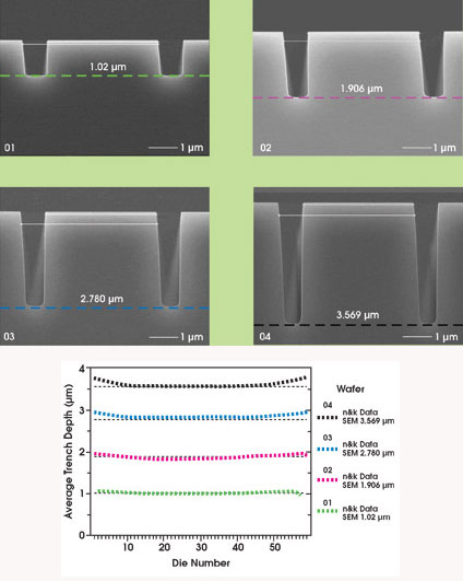
Figures 2 and 3. Comparative
measurements of a series of trench systems indicate that average trench depths measured
by broadband spectrophotometry agree with SEM trench measurements. Spectrophotometric
data also reveal distinct center-to-edge variations and readily distinguish trench
geometry process variations on the order of 100 Å. Although this level of
wafer uniformity, or lack thereof, would be difficult and time-consuming to detect
using conventional techniques, broadband spectrophotometry supported by a valid
physical model makes it available within minutes, indicating that the method is
well-suited for enhancing manufacturing production.
Conversely, broadband spectrophotometry
based on the Forouhi-Bloomer equations can nondestructively map an entire 300-mm
wafer in minutes, returning average results from a measurement spot size ranging
from 50 μm to 1 mm, depending on the configuration of the system. Besides accurately
measuring standard quantities like trench depth and width, the system also can acquire
a wealth of data regarding the thicknesses and properties of films deposited inside
and outside of trench regions.
The semiconductor industry has begun
applying phase-shift masks to reduce feature sizes and to squeeze the most potential
out of optical lithography. This makes characterization of phase-shift materials
and masks one of the most important and immediate needs for accurate measurement
technology. Instruments also must measure transmittance through both the phase-shift
material and the substrate at specified wavelengths as well as the film parameters.
Specifically, the characterization data must confirm that a mask delivers the ideal
phase-shift of 180° as well as specified transmittance in the 5 to 10 percent
range.
Because smaller critical dimensions
typically rely on shorter exposure wavelengths, it is important to adequately characterize
film structures at deep-UV wavelengths. Currently, deep-UV dual-beam laser interferometry
provides direct measurements of phase-shift materials and masks. However, this type
of tool is expensive and is effective at only one wavelength. In addition, it obtains
measurements after the mask has been patterned, thus diminishing the possibility
of detecting poor mask characteristics prior to patterning. Finally, these interferometers
are slow, making mapping inherently difficult.
Broadband spectrophotometry supported
by the Forouhi-Bloomer equations simultaneously measures reflectance and transmittance
at the same point to determine phase shift, film thickness and the values of n,
k and Eg. As demonstrated on a patterned phase-shift mask (Figure
4), the technology can quickly provide a multiple-point map of reflectance and transmittance
spectra of a MoSiOxNy film on a quartz substrate. It also can detect nonuniformities
in phase shift not only for patterned films, but for blanket films as well. This
is particularly important because uniformity of phase-shift masks must be tightly
controlled. Other applications require control of phase shift better than ±1°
over the entire mask.
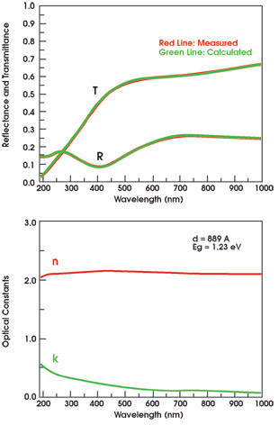
Figure 4. Broadband spectrophotometry can provide a 49-point map of reflectance and transmittance
spectra of a MoSiOxNy film on a quartz substrate in about 1.5 minutes. Here is represented
the experimental and calculated reflectance and transmittance spectra (top), simultaneously
measured at the same point of a patterned phase-shift mask. Thickness (d), n and
k spectra and Eg appear in the bottom graph.
Broadband spectrophotometry based on
these equations can also characterize free-standing SiNx membranes used for Scalpel
electron-beam lithography, a promising next-generation lithography technology. Some
of the meaningful data obtained for electron-beam techniques includes thickness
of the SiNx membrane, values of n and k in the deep-UV and transmittance through
the membrane in the deep-UV. This information helps control the process of making
the Scalpel mask and determining its uniformity.
Much data, single measurement
The clear advantage of broadband spectrophotometry
is that a single, multiple-wavelength optical measurement can determine many more
parameters and film characteristics than can be obtained from instruments designed
for specific direct measurements. Spectrophotometric results based on Forouhi-Bloomer
equations compare favorably with those obtained using more time-consuming methods;
namely, profilometry, AFM and spectroscopic ellipsometry. Also, spectrophotometric
measurements are fast, simply made, accurate, repeatable and reproducible. The instrumentation
is easily incorporated with fabrication equipment, making it ideal for process control.V=
The margin for error is shrinking in
the manufacture of microelectronic devices and components. As a consequence, demand
is growing for greater inspection frequencies and more accurate, rapid, nondestructive
and low-cost characterization tools for process development and control. Also, successful
metrology tools must provide stable and consistent measurements when faced with
normal variations in the manufacturing process. Lastly, new measurement techniques
must quickly and accurately determine characteristics such as thickness and uniformity
of thin and ultrathin films and to ensure that their integrity is not jeopardized.
Broadband spectrophotometry meets and
exceeds the metrology requirements that are necessary to produce high-quality and
high-performance protective coatings.
Meet the authors
Iris Bloomer is executive vice president and co-founder
of n&k Technology Inc. in Santa Clara, Calif.
Rebecca Mirsky, a senior technology
writer for Al Shugart International, is based in Boise, Idaho.
The Enabling Algorithm
With an appropriate physical model to represent the index of refraction (n) and the extinction
coefficient (k) of a thin-film material, broadband spectrophotometry can quickly
and nondestructively analyze the thickness and optical properties of the film. Equations,
developed by A.R. Forouhi and Iris Bloomer, constructed a physical model for n and
k in terms of wavelength and material parameters, enabling accurate thin-film characterization
simply by measuring reflectance.
The model is applicable to a wide range of semiconductor
and dielectric films and fits experimental data over the deep-ultraviolet through
the near-infrared wavelength range.
The Forouhi-Bloomer equations are given by:
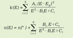 In these equations, E is the
photon energy related to the wavelength of light according to E = hc/λ, where
h is Planck’s constant and c is the speed of light in a vacuum. Eg
is the energy bandgap, and A, B and C are related to the electronic
structure of the material. The quantities Bo and Co
are not independent parameters, but depend on A, B, C and Eg.
In these equations, E is the
photon energy related to the wavelength of light according to E = hc/λ, where
h is Planck’s constant and c is the speed of light in a vacuum. Eg
is the energy bandgap, and A, B and C are related to the electronic
structure of the material. The quantities Bo and Co
are not independent parameters, but depend on A, B, C and Eg.
Equation 2, for n(E),
is derived from equation 1, for k(E), through the Kramers-Kronig dispersion
relation.
Both equations can describe amorphous
materials by taking only one term in the sum; that is, by taking the integer q
to be equal to one. They describe polycrystalline and crystalline materials by taking
the integer q to be equal to two or more.
References
1. A.R. Forouhi and I. Bloomer (1986). Optical
dispersion relations for amorphous semiconductors and amorphous dielectrics. Physical
Review Letters B. Vol. 34, p. 7018.
2. A.R. Forouhi and I. Bloomer (1988).
Optical properties of crystalline semiconductors and dielectrics. Physical Review
Letters B. Vol. 38, p. 1865.