Fabrication of semiconductor devices inside microstructured optical fiber may lead to all-fiber optoelectronics.
John V. Badding and Venkatraman Gopalan, Pennsylvania State University, and Pier J.A. Sazio, University of Southampton
The backbone of the information superhighway comprises optical fiber. Optical fiber technology has lead to the revolution in telecommunications and is affecting many other fields, from defense and remote sensing to biomedicine. This impact is growing in part because of rapid advances in active fiber devices for which the fiber serves not only as a passive waveguide, but also as a medium to directly modulate, generate or otherwise manipulate optical radiation.
In addition, the pervasive nature of electronics and optoelectronics technology based on silicon, GaAs and other crystalline semiconductors is familiar to almost all scientists and engineers.
These two technologies — namely, fiber optics based on long thin strands of glass and electronics based on planar chips fabricated by lithography — typically are heterogeneously interfaced through intermediate optics and packaging. Modern telecommunications, for example, uses both planar optoelectronic semiconductor devices (e.g., lasers, modulators and detectors) and silica optical fiber. However, wherever possible, it is desirable to avoid transforming in-fiber photonic signals to chip-based electronic signals and back again because of the cost and complexity incurred by such optical-electronic-optical or optical-electronic conversions. An approach that does not require the photons to leave the fiber would be preferable.
The ultimate vision in this quest is all-fiber optoelectronics in which most, if not all, of the functions currently performed by heterogeneous, discrete and, therefore, expensive electronic components are performed inside the glass fiber (Figure 1). The erbium-doped fiber amplifier (EDFA), for example, has revolutionized telecommunications because it enables in-fiber amplification of many densely multiplexed wavelengths without the difficulties associated with electronically detecting, amplifying or regenerating those wavelengths outside the fiber. Although the EDFA has solved the problem of how to amplify the 1.5-μm radiation used for telecommunications, heterogeneous optical-electrical-optical conversions still are required for other essential functions, such as reshaping and retiming the digital pulses. These conversions remain a major cost for optical networks.
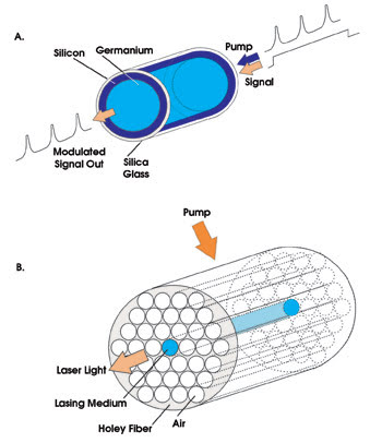
Figure 1. Incorporating semiconductors into optical fiber enables a number of all-fiber optoelectronic concepts, including an in-fiber optical modulator in which the pump modulates the refractive index of a silicon core and, thus, the amplitude of a guided signal at a different wavelength (A) and a fiber laser based on an optically pumped semiconductor gain medium (B).
Our team recently demonstrated that long semiconductor and metal tubes, wires and heterojunctions can be fabricated inside optical fibers via a deposition process similar to that used for modern planar electronic devices.1 This new approach opens the possibility for directly combining the flexible waveguiding capabilities of an optical fiber and the exceptional capabilities of semiconductors and metals for manipulating optical radiation and electrons.
As a proof of principle, we made a field effect transistor composed of crystalline germanium inside a fiber. This innovation suggests that many of the functions performed by planar optoelectronics may be integrated into fiber and that new semiconductor devices that cannot be realized in a conventional planar geometry may become possible. The result may be low-cost, highly functional devices that seamlessly integrate with the fiber-based infrastructure.
Building inside fiber
Because semiconductors such as silicon and the silica glass used for telecom fiber have different physical properties at high temperatures, it has not been possible to draw them together into a high-quality fiber. This incompatibility is an excellent example of how the properties of materials strongly constrain what is technologically possible.
The alternate paradigm that we have developed is to build electronics inside microstructured optical fibers, which are a topic of intense current research in photonics. In contrast to conventional fibers with solid cores, microstructured optical fibers are typically drawn with tiny capillary airholes ranging from tens of nanometers to a few microns in diameter running along their entire length. (“Solid” microstructured optical fibers, in which the airholes are replaced by different types of glass, also can be made.) Hundreds to thousands of such capillary holes can be precisely engineered into complex, highly regular patterns within the cross section of a single optical fiber (Figure 2).
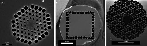
Figure 2. Scanning electron microscopy shows cross sections of solid-core microstructured optical fibers (A and B) and hollow-core photonic bandgap fiber fabricated at the University of Southampton (C).
Microstructured optical fibers can be divided into two classes: 1) those that guide light via a modified form of total internal reflection resulting from the array of airholes acting as a cladding layer with lower average index of refraction than the solid core and 2), those that rely on a photonic bandgap in the cladding to confine the light to the core, often termed photonic bandgap fibers. The ordered arrangement of holes in such fibers gives rise to a photonic bandgap just as the ordered arrangement of atoms in a silicon crystal gives rise to the more familiar semiconductor electronic bandgap. The fibers in Figures 2A and 2B have solid cores and were designed to guide light via total internal reflection.
Hollow core fibers such as that shown in Figure 2C, on the other hand, guide via photonic bandgap effects. They have a core whose refractive index is lower than that of the cladding. The air core, in this case, acts as a defect level inside such a photonic bandgap, similar to the defect levels introduced inside the electronic bandgap of a silicon crystal through doping. Solid-core fibers can be designed to guide via photonic bandgap effects as well.
The most interesting aspect of microstructured optical fiber for us, however, is that the holes provide a way to infiltrate other materials into the fiber.
The conventional means of fabricating layers of semiconductors for planar devices is chemical vapor deposition. A chemical precursor in gaseous form is heated to decompose it so it will form a layer of the desired material on the substrate. For silicon, the most common precursor is silane (SiH4). When heated, silane gives up its hydrogen and can form pure, crystalline layers of silicon. Many different semiconductors can be deposited by choosing the appropriate precursor. For example, germane (GeH4) decomposes into germanium, and more complex precursors are known for many of the direct-bandgap compound semiconductors such as GaAs and InP.
Given the experience with chemical vapor deposition technology accumulated over more than 50 years, it would seem to be an obvious method for fabricating semiconductor structures within microstructured optical fiber, but this turns out to be rather challenging. The holes in the fiber are centimeters to meters long (or even longer), but they may be less than 100 nm in diameter — a dimension approaching the smallest sizes used in production lithography of semiconductor devices. Any layer of semiconductor that forms along the walls of features with such an extreme aspect ratio (106 or greater) would have to be nearly perfectly smooth and conformal, or a plug would form that would arrest further deposition. Moreover, the rate of flow of the precursor into a hole so small and so long would be slow and, as a result, little material could be deposited in a practical amount of time.
Accordingly, we developed the alternative technique of high-pressure microfluidic chemical vapor deposition. We found that we could use the empty holes in microstructured fiber as micro- to nanoscale reaction chambers for the deposition process if we used precursor pressures in the range of 100 to 1000 bar, at which the gases are sufficiently dense that they behave like fluids.
For example, a mixture of germane gas and an inert carrier gas can be configured to flow through the pores of a microstructured fiber that is being heated to several hundred degrees. This temperature is sufficient to decompose the germane into germanium along the walls of the holes. The deposition is surprisingly smooth and is conformal over lengths of centimeters to tens of centimeters. Because the volume of the holes is so small, the high pressures present little or no safety hazard. Figure 3A shows a smooth tube of germanium fabricated inside a single 1.6-μm-diameter hole of a microstructured optical fiber. The process works so well that it is possible to fill the holes almost entirely (Figure 3B).
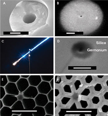
Figure 3. A scanning electron microscope image reveals the cross section of a germanium tube inside a microstructured optical fiber (A). The scale bar is 500 nm. Another micrograph shows a germanium wire inside a fiber (B). The scale bar is 200 nm. In this bundle of germanium wires emanating from a microstructured fiber, blue laser light propagates down the silica fiber cladding but not the wires (C). A micrograph shows a nanoscale germanium wire inside a microstructured optical fiber (D). The scale bar is 100 nm. An unfilled honeycomb template (E) and the template after filling with germanium (F) are shown. The scale bar is 5 μm in both instances. Images reprinted with permission of Science.

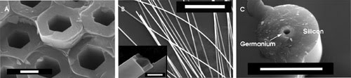
Figure 4. A scanning electron microscope exposes the cross section of silicon tubes in honeycomb fiber (A). The scale baris 1 μm. Such tubes may be etched out of honeycomb fiber using hydrofluoric acid (B). The scale bar is 100 μm. A close-upreveals the shape of the tubes imposed by a honeycomb template (B, inset). A Si/Ge annular heterojunction was fabricatedinside the hole of a microstructured optical fiber (C). The scale bar is 6 μm. Images reprinted with permission of Science.
Similar results have been obtained for silicon wires (Figures 4A and B), and we anticipate extending the variety of materials that can be fabricated inside the fiber to include compound semiconductors such as GaAs and InP. We have deposited a range of other materials, including compound semiconductors such as GeS2, Si-Ge alloys and oxides, and metals such as gold and platinum. By sequentially varying the precursor, semiconductor/semiconductor or semiconductor/metal heterojunctions can be fabricated (Figure 4C). Gold and silicon also have been patterned along the length of the holes by focusing a laser to heat or photochemically decompose a precursor (Figure 5).
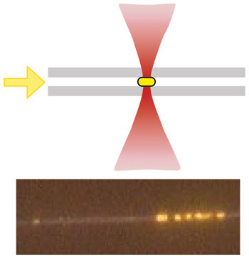
Figure 5. Focused laser radiation (red) enables the deposition of semiconductor or metal from flowing precursors (yellow arrow) at precise locations along the length of a capillary hole (top). Gold particles are deposited in a pattern within a microstructured optical fiber capillary (bottom; reprinted with permission of Science).
For some applications, the superior electron transport and photonic properties of single-crystal semiconductors will be necessary. Single-crystal silicon wires have been nucleated and grown via a technique that uses a liquid gold/semiconductor particle that travels along the length of the hole, depositing single-crystal silicon behind it.
All of these structures can be viewed as basic building blocks for devices, and many more sophisticated structures can be envisioned via the straightforward extension of the techniques developed to date.
As a demonstration of electronic functionality inside an optical fiber, we have fabricated a semiconductor field effect transistor inside a fiber (Figure 6). Doing so enables us to directly measure and compare relevant semiconductor parameters such as carrier type, concentration, mobility and activation energy to standard values for silicon and germanium.
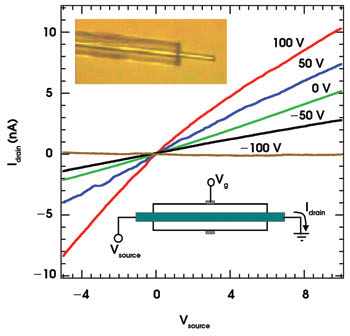
Figure 6. A germanium field effect transistor was integrated into a fiber. An optical micrograph reveals the germanium wire protruding from silica fiber after etching (inset, top). A circuit diagram depicts the in-fiber field effect transistor (inset, bottom). The plot shows the source-drain current for different values of bias voltage (Vg ). Reprinted with permission of Science.
Moreover, if the carriers in a semiconductor material have high mobility, there will be few defects, and the optical properties also will be excellent. Thus, the field effect transistor not only provides an important proof of principle of in-fiber electronic devices, but also is a valuable characterization tool.
New functionalities arise from the patterns of holes within the fiber that can be filled as well as from the longitudinal structuring possible by our photoinitiated patterning technique. The refractive indices of semiconductors such as silicon (n = 3.5) and germanium (n = 4.0) are much larger than that of the silica matrix (n ≈ 1.5). Therefore, the optical characteristics of microstructured optical fiber can be heavily modified, and radiation can be manipulated at dimensions down to the nanoscale.
For example, the photonic bandgap and the optical dispersion characteristics can be altered significantly by coating the holes inside the fiber with annular tubes or rods of semiconductors such as silicon. The thickness of a tube controls the number of guided modes very sensitively. For perspective, although a conventional solid-core, single-mode silica optical fiber has a core diameter of many microns, one needs only ~50 nm of silicon core inside a silica capillary fiber for single-mode guidance.
‘Salami photonics’
A majority of nanophotonic devices today — from passive waveguides, filters and photonic crystals to active resonator and modulator devices — are made in planar geometries through state-of-the-art electron-beam lithographic techniques. Even so, creating a two-dimensional array of a photonic crystal composed of silicon nanopillars with air matrix on a planar geometry requires deep ion-beam etching, which limits the pillar height to a few tens of microns.
Our technique provides an alternate method that is attractive in many respects. Once a single silica fiber with thousands of prearranged holes has been filled with a high-index semiconductor such as silicon, it may be viewed as a 2-D photonic crystal from the side (Figure 7). The fabrication does not require high-end, time-consuming lithographic techniques; it is simple and rapid. In addition, the extreme lengths of the semiconductor structures provide aspect ratios that are virtually unlimited.
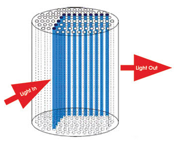
Figure 7. Two-dimensional photonic crystal devices can be fabricated by sectioning lengths of filled microstructured optical fiber — a process called“salami photonics.
We call this concept “salami photonics” because the long length of the filled fiber can be sliced, salamilike, into a large number of 2-D photonic crystal devices. Bundles of these fiber sections can be used to scale up laterally the size and the symmetry.
Fiber lasers, both pulsed and continuous, are already a commercial reality. Typically, these lasers use rare-earth-doped glasses as optically pumped gain media and the fiber itself as a laser cavity to build up gain. They are typically restricted to near-infrared wavelengths in the 0.8- to 2-μm range. Semiconductor lasers, in contrast, greatly expand the availability of wavelengths, from the visible (e.g., AlGaN, GaAs and AlGaAs) to the near-infrared (e.g., InGaAsP) and beyond into mid- and long-infrared wavelengths (e.g., PbS, PbSe, GeS2, HgCdTe). In-fiber electrical pumping of the laser medium could be achieved using PN heterojunctions, which we can fabricate as annular or axial junctions within the microstructured fiber. Optical pumping also is possible.
Another clear advantage that semiconductors have over fiber lasers is that the second- and third-order nonlinear effects are many orders of magnitude larger than the corresponding parameters in optical glasses. Thus, nonlinear phenomena such as three- and four-wave mixing, and stimulated Raman and stimulated Brillouin scattering can be exploited for optical frequency conversions for optical communications.
Semiconductor detectors are ubiquitous (e.g., Si, Ge, InAsP and HgCdTe) in the optoelectronics industry, based on effective electronic bandgap selection and engineering to detect various photon energies. Photons typically are absorbed by the semiconductor at a PN junction, and the created electrons and hole are swept away under a reverse bias, providing an electrical signal. Axial and radial PN junctions can be created inside the holes of the microstructured optical fiber, and electrical contacts to them also can be provided by directly depositing metal tubes as contacts.
The technology we have developed represents a platform for fiber-based optoelectronics of unprecedented sophistication that could be robust, inexpensive and seamlessly integrated into the existing fiber-based infrastructure. To fully realize the promise of all-fiber optoelectronics, continued development of the materials deposited within the fiber will be necessary, just as early-stage low-loss silica fiber technology required considerable evolutionary materials development. Thus, our current focus is on performing the fundamental materials science that is necessary to develop these novel structures for application in the next generation of photonic devices.
Meet the authors
John V. Badding is an associate professor of chemistry at Pennsylvania State University in University Park; e-mail: [email protected].
Venkatraman Gopalan is an associate professor of materials science and engineering at Penn State; e-mail: [email protected].
Pier J.A. Sazio is senior research fellow at the University of Southampton’s Optoelectronics Research Centre in the UK; e-mail: [email protected].
Acknowledgments
V.G. and J.V.B. thank the National Science Foundation (grant DMR-0502906), the Penn State Center for Nanoscale Science, funded by NSF grant DMR-0213623; and the Penn State-Lehigh Center for Optical Technologies for support.
Reference
1. P.J.A. Sazio et al (March 17, 2006). Microstructured optical fibers as high-pressure microfluidic reactors. SCIENCE, pp. 1583-1586.