CCDs continue to be the sensor of choice for applications such as astronomy and spectroscopy. With future investment, we can expect improvements in sensor architecture, resolution, pixel size and depth, as well as readout speeds.
Over the last few decades charge-coupled device (CCD) sensors have been slowly overtaken by CMOS sensors for applications ranging from mobile phone cameras to surveillance. But CCDs still have a lot to offer, particularly where extreme sensitivity and long exposures are crucial. And if their price continues to drop without compromising performance, CCD technology will be an appealing option for broader mid-market applications.
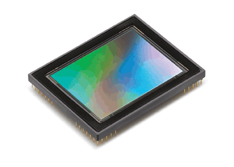
Teledyne Dalsa offers powerful, innovative CCD and CMOS sensors for any application, from visual to near-IR to hyperspectral and beyond. Photo courtesy of Teledyne Dalsa.
Combining ultimate sensitivity with low readout noise made the CCD sensor a staple in the imaging sector for over
30 years. In fact, for the last 20 years, the Sony ICX285 sensor was used almost universally across scientific, industrial and surveillance applications.
However, CMOS technology has enjoyed the most dramatic improvements in the past few years and now offers the benefits of resolution, speed and noise, as well as price. The result is a shift toward CMOS by many markets, particularly the life sciences, consumers, some industrial sectors and surveillance.
“Companies like BAE (formerly Fairchild Imaging), CMOSIS and Sony have invested heavily in their CMOS technology and pushed a very strong marketing message that CMOS offers the best combination of speed, resolution and sensitivity,” said Mark Donaghy, vice president of sales and marketing at Raptor Photonics Ltd. in Larne, Northern Ireland, a manufacturer of low-light-level digital cameras. “You now see sensors that are 4 MP or larger, running at 50+ fps with only a few electrons read-out noise.”
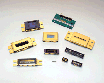
A lineup of image sensors from Hamamatsu Photonics. Photo courtesy of Hamamatsu Photonics.
But for applications where extreme sensitivity is crucial, especially for longer exposures, a CCD sensor remains the best option. In areas such as in vivo imaging that rely on very weak fluorescence signals on exposures of several minutes or even hours, cooled CCDs work best, as they offer very low dark current. Similarly, for astronomy applications where longer exposures are used for gazing, cooled CCDs once again offer the best option.
Extending wavelength sensitivity
There is growing demand for CCD sensors to improve their sensitivity over a broader wavelength range. Today, significant advances are being made to improve the spectral response performance in UV and near-IR regions through a combination of back-thinning and various sensor processing techniques. In fact, new technologies could be key to opening up CCDs for use in near-IR applications for up to 1100 nm.
“Their lack of sensitivity beyond 1100 nm limits their applicability in the short-wave infrared (SWIR) regime. The latest generation indium gallium arsenide (InGaAs) detectors are preferred in this region,” said Ravi Guntupalli, vice president of sales and marketing at Princeton Instruments, specialists in scientific imaging and spectroscopy with global offices. “These sensors use CMOS like readout and are capable of high speeds and high sensitivity when they are deeply cooled.”
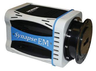
The latest EMCCD from Horiba Scientific. Photo courtesy of Horiba Scientific.
The aim is to improve quantum efficiency in these spectral regions and minimize the adverse phenomenon of etaloning – an interference effect where light is continuously reflected between the front and back surfaces of a CCD.
EMCCDs
Electron Multiplying CCDs, or EMCCDs, grew in popularity to become an industry favorite a few years ago, presented as the most sensitive sensor technology available. Sensor manufacturers such as e2v Technologies PLC of Essex, UK, and Texas Instruments Inc. of Dallas, are providing sensors capable of delivering sub-electron readout noise with faster speeds, while ON Semiconductor Corp. of Phoenix, Ariz., has developed a new range of high-definition EMCCD sensors.
“It took the imaging market by storm and a number of leading researchers were able to use this technology to see things they have never been capable of seeing before. However, resolution, pixel size and cost were the limiting factors,” Donaghy said.
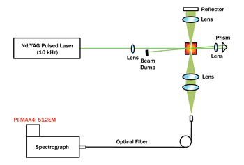
Experimental apparatus showing a high-speed laser Raman diagnostic system employing an Nd:YAG pulsed laser (532-nm, 88-ns pulse width, 10-kHz repetition rate) and a Princeton Instruments PI-MAX4: 512EM emICCD camera coupled to a lens spectrograph. Photo courtesy of J. Kojima, OAI/NASA.
Princeton Instruments recently launched a line of high-speed EMCCD cameras capable of single photon sensitivity and imaging speeds of up to 10,000 fps. The capabilities are further enhanced by coupling these sensors to image intensifiers to improve linearity and provide single photon sensitivity with subnanosecond gating times.
“For example, researchers at NASA’s Glenn Research Center use these new-found capabilities to perform time-resolved spontaneous Raman scattering (SRS) to analyze combustion processes at molecular level,” Guntupalli said.
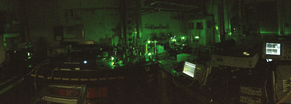
Dr. Jun Kojima of the Ohio Aerospace Institute tests the new Raman spectroscopy technique at NASA’s Glenn Research Center. Photo courtesy of J. Kojima, OAI/NASA.
While such EMCCDs can provide single photon sensitivity, they cannot match the frame rates of CMOS sensors at full resolution. However, advances in readout techniques do enable them to achieve multikilohertz frame rates, albeit at reduced resolution.
Spectroscopic instrument maker Horiba Scientific in Edison, N.J., a division of Horiba Instruments Inc. of Irvine, Calif., is finding demand continues to grow from formerly niche spectroscopic and imaging techniques that have begun to gain increasing acceptance as standard methods in many fields.
“What were formerly research instruments and methods are increasingly being used for more generic purposes such as quality control, etc.,” said Dr. Francis Ndi, export manager at Horiba Scientific. “This growth is also driven by the demands for higher throughput, so that methods that previously used single channel detectors are now using the multiplexing offered by array detectors such as CCDs to increase the measurement throughput.”
Another driver of CCD advances is technology for adjusting the intrascenic dynamic range – primarily useful for imaging applications with uncontrolled lighting or very bright and very dark objects in the same frame.
“Significant resources are also being spent on efforts to improve yield and drive down cost for some of the higher-end chips, which is an enabler for entry into some of the mid-market bench top spectroscopy and imaging applications,” Ndi continued. “A lot of work is also being done with on-chip spectral filtration for hyperspectral and multispectral applications.”
Time delay integration CCDs
When users call for measurements to be made faster but without compromising sensitivity, time delay integration (TDI) CCDs are the answer. Crucially, this is one key CCD capability that earlier versions of CMOS imagers simply cannot replicate.
TDIs are commonly used in industrial and remote sensing applications to enhance the signal-to-noise ratio when imaging at very high speeds. TDIs have the ability to sum signals captured at different time intervals, and by charge summing, superior noise performance can be achieved.
In CCDs, signal charges are summed, while in conventional CMOS imagers, signal voltages are summed.
Different companies have been working on their own approaches to integrate charge-domain TDI with CMOS. According to Nixon O, technical director of imaging R&D at machine vision specialist Teledyne Dalsa Inc. in Ontario, Canada, some integrate CCD photosites within the CMOS imager; others fabricate the CCD photosites and CMOS readout chips separately, and connect the CCD to CMOS using 3DIC (three-dimensional integrated circuit) hybridization techniques.
“For industrial and remote sensing applications that require TDIs, we expect to see a migration to one of these hybrid CMOS-CCD imagers,” Teledyne’s O said.
“At Teledyne Dalsa, we continue to work on new processes that enhance the low-light sensitivity, radiation stability and spatial resolution of imagers, particularly for wavelength ranges outside the visible spectrum,” he said. “Most of these processes are applicable to CMOS, CCD and CMOS-CCD hybrids. We also spend a significant effort ensuring that our new processes maintain high yields (and hence low cost), even as the new advances make the devices more difficult to manufacture.”
Hamamatsu Photonics’ range of TDI CCDs allow users to synchronize the charge transfer through the CCD without moving the object being imaged. This enables them to achieve extremely fast frame rates (typically around 100k frames per second).
“One of the research areas uses TDI to satisfy the requests for higher frame rate,” said Craige Palmer, general sales manager at Hamamatsu Photonics U.K. Ltd. “The other area is increasing the range of back-
thinned and deep-depletion CCDs to achieve higher quantum efficiency.”
CCD sensors are more than holding their own in high-end spectroscopy and imaging applications. If the technological advancements that drive down cost can be achieved without significant sacrifices in performance, then Horiba’s Ndi believes that this will spur adoption of existing niche techniques into broad mid-market applications, while increasing use in non-research environments.
The Business of CCDs: At a Glance
While CCD and CMOS are separate technologies, they do share common processes, and so many expect that the two will have intertwining paths in the future.
The gradual switch from CCDs to CMOS across many markets means that today, CMOS imagers outsell CCDs.
A particularly momentous turning point in the imaging sensor market occurred when mobile phone cameras switched to CMOS imagers. From this moment on, enormous investment was made to develop, fine tune and perfect the technology and the fabrication processes that manufacture CMOS sensors. As a result of this investment, great strides have been made in image quality, even as pixel sizes shrink.
Sony’s recent decision to discontinue the design and manufacture of CCD sensors in March 2017 – switching its focus instead to the development of CMOS sensors – sent shock waves through the sensor market. But, realistically, this should be no surprise given that Sony’s biggest markets are industrial and surveillance, which are more suited to the larger resolutions and faster speeds that CMOS is capable of delivering.
The top applications currently driving forward advances in CCD sensor technology include:
1. Spectroscopy (Raman, fluorescence, photoluminescence)
2. Hyperspectral imaging
3. Biomedical imaging (e.g., blood analyzers)
4. Microscopy
5. Astronomy
6. Quantum imaging
7. X-ray imaging
8. Machine vision (including color sensing)