
CEA-Leti, Intel Advance Die-to-Wafer Self-Assembly Process
SAN DIEGO, June 6, 2022 — CEA-Leti reported the optimization of a hybrid direct-bonding, self-assembly process with the potential to increase the alignment accuracy as well as fabrication throughput of die-to-wafer (D2W) bonding. The work is part of a collaboration with Intel.
The progress is described in a paper presented at the 2022 Electronic Components and Technology Conference, titled “Collective Die-to-Wafer Self-Assembly for High Alignment Accuracy and High Throughput 3D Integration.” The paper describes a process using the capillary forces of water to align the dies.
Photonic applications, as well as those involving memory and high-performance computing, are among those supported by the self-assembly process, CEA-Leti said.
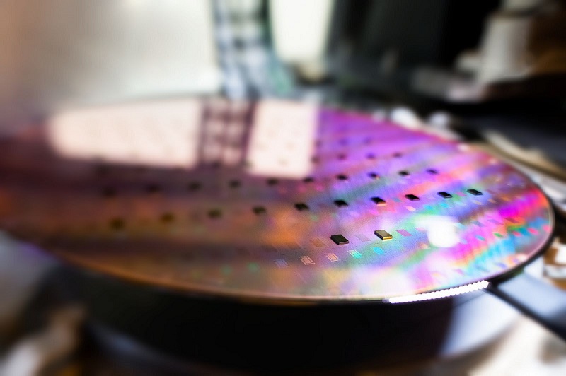
CEA-Leti and Intel reported progress on a die-to-wafer self-assembly process. Courtesy of A. Aubert/CEA-Leti.
“Commercial-scale throughput with D2W self-assembly presents two main challenges related to die handling,” said Emilie Bourjot, CEA-Leti’s 3D integration project manager. “If the self-assembly process is combined with a pick-and-place tool, the throughput can be increased by reducing the time of alignment, since the fine alignment is performed by the droplet. When self-assembly is combined with a collective die-handing solution, the throughput is increased by the fact that all dies are bonded together at the same time without any high-precision placement at any time along the process flow.”
Process optimization is also an important part of this work for increasing process maturity and targeting industrial requirements.
This mechanism described in the paper allowed the self-alignment of the die on its bonding site. “The liquid chosen as the realignment vector must present a high surface tension and has to be compatible with direct bonding,” the paper said.
Water, which has a surface tension of 72.1 mN/m, stood out as a prime candidate, as most liquids have a surface tension between 20 and 50 mN/m.
“The water dispense technique and the surface preparation to tune the surface hydrophilicity appeared as critical for the proper conduct of the self-assembly process,” according to the paper. “Thus, excellent alignment performance on a homemade collective self-assembly bonding bench was achieved.”
The team fabricated its own lab bench enabling a collective self-assembly due to the lack of industrial tools in existence to support the assemblage. The process achieved alignment of 500 nm and below, which indicated that an industrial tool dedicated to this process would deliver higher reproducibility, robustness, and precision, according to the paper.
/Buyers_Guide/CEA-Leti/c24495