
CEA-Leti Names CEO
GRENOBLE, France, July 1, 2021 — The technology research institute CEA-Leti named Sebastien Dauvé CEO, effective July 1. Dauvé succeeds Emmanuel Sabonnadière, who had served as CEO since November 2017. Dauvé joined CEA-Leti in 2003. In 2016 he became director of the institute's Systems Division.
Sabonnadière has been appointed to the newly created position of vice president silicon carbide (SiC) program at Soitec, a designer and manufacturer of semiconductor materials.
Soitec announced the appointment on July 1.
In a press release, Dauvé said, “Hardware is definitely back in the tech industry spotlight: From MedTech, power electronics for e-vehicles, to telecommunication networks and IoT, the semiconductors play an ever-larger role in our society.
“CEA-Leti multidisciplinary teams have a solid technological expertise coupled with advanced platforms to help make the necessary shift towards sustainable electronics, while continuing on delivering greater performance, downsizing form factor, and lowering cost.”
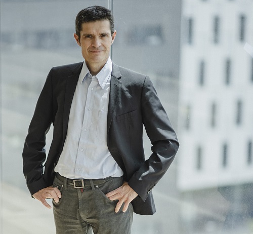
Sebastien Dauvé has been named CEO, succeeding Emmanuel Sabonnadière. Courtesy of CEA-Leti.
As CEA-Leti’s CEO, Dauvé leads the activities of one of Europe’s largest micro- and nanotechnologies research institutes, which employs 1900 scientists and engineers, has a portfolio of 3000 patents, and has launched more than 70 startups.
Dauvé previously served as a laboratory manager at CEA-Leti, then head of an R&D department that specialized in sensors applied to the IoT and e-mobility. In that position, he supported the dissemination of new technologies in industry, including the automotive industry, aeronautics and national defense, and microchips.
Soitec was founded in 1992 and was developed in collaboration with CEA-Leti. In 2018, the two launched a substrate innovation center to develop engineered substrate solutions. In 2019, Soitec announced its joint development program with Applied Materials, a supplier of equipment, services, and software for the manufacture of semiconductor chips for electronics on next-generation silicon carbide substrates. In announcing the development program, the companies said that they will install a silicon carbide engineered substrate pilot line at the Substrate Innovation Center, which is located at CEA-Leti. The program aims to provide technology and products to improve the performance and availability of silicon carbide to address surging demand from electric vehicles, telecommunications, and industrial applications.
/Buyers_Guide/CEA-Leti/c24495
/Buyers_Guide/Soitec/c13786
/Buyers_Guide/Applied_Materials/c989