
CMOS Imaging: From Industry to Consumer and Back Again
Ongoing advancements in CMOS sensor design are creating new possibilities for all sides of the imaging industry.
ERIC FOX, TELEDYNE DALSA
Technology often advances unnoticed. Incremental improvements may only be seen by insiders in industries that a technology already calls home. Sometimes it achieves a breakthrough point and whole societies can change as a result. This often happens in the consumer space, where big budgets and large consumer bases help turn “toys” into real productivity tools for some of the most exciting industries — such as manufacturing inspection, food safety, security, medical and health, metrology, and mapping.
Looking forward with CMOS technology, applications for industrial and consumer users will continue to drive advancements, ultimately benefitting both sectors.
Driving innovation
The entire sensor industry is surging, according to reports by market research firms Energias Market Research, and Research and Markets. The global image sensor market, in particular, is expected to grow significantly, from $14.1 billion in 2017 to $25.6 billion in 2024, at a compound annual growth rate of 10.3 percent. The majority of this growth will occur in the consumer space, which typically commands nearly 80 percent of the market.
Consumer applications involving CMOS have largely centered on human vision, particularly in relation to mobile phone cameras. This means area-scan, visible-spectrum, low-power, low-cost, small-package sensors will make up the majority of the market. These characteristics are all virtues touted by phone manufacturers as competitive advantages in this cutthroat and lucrative industry.
The industry therefore drives tremendous advancements in CMOS image sensor technology — smaller pixels, lower-noise circuits, backside illuminated photodiodes, and new silicon manufacturing processes such as deep submicron fabrication. As the market becomes saturated, companies are also looking at new possibilities for growth. 3D image sensors have positioned themselves within the fastest growing market, thanks to new applications in machine vision — specifically robotics.
High-speed, high-precision assembly robots are only possible when they have vision systems that match. While machine vision was at the forefront of the development of 3D imaging technologies, it’s the consumer world that has found high-volume uses for 3D imaging and continues to be its biggest driver — in automotive (advanced driver-assistance systems), gaming (gesture recognition), and mobile devices (proximity sensors).
Nonvisible spectra — hyperspectral, multispectral, and polarized — are also expected to experience some of the highest growth, driven by medical, automotive, consumer electronics, and industrial applications.
Striving for high speed
In consumer spaces, higher speed and resolution have helped manufacturers sell new phones, digital single-lens reflex (DSLR) cameras, and cinema cameras. In the industrial space, such improvements have enabled higher quality control and more efficiency. These advancements are possible because designers have consistently been able to make CMOS sensors image faster. But the higher resolutions and faster speeds now exceed 5 gigapixels/s, causing complex engineering problems when managing the flow of data.
At the sensor level, this data flow requires faster interfaces and more parallel data paths. Each output runs faster. Today, clock speeds run at an order of magnitude faster than just a few years ago, from 100 MHz then to several gigahertz now.
High speed and high resolution necessarily come with high data rates. The need to transmit and process all of this data puts pressure on all three fronts of imaging-system design: sensor, data pipe, and processing. All need to expand in concert, with the help of higher-performing tools such as frame grabbers (Figure 1), to avoid compromising on this new high-speed paradigm.
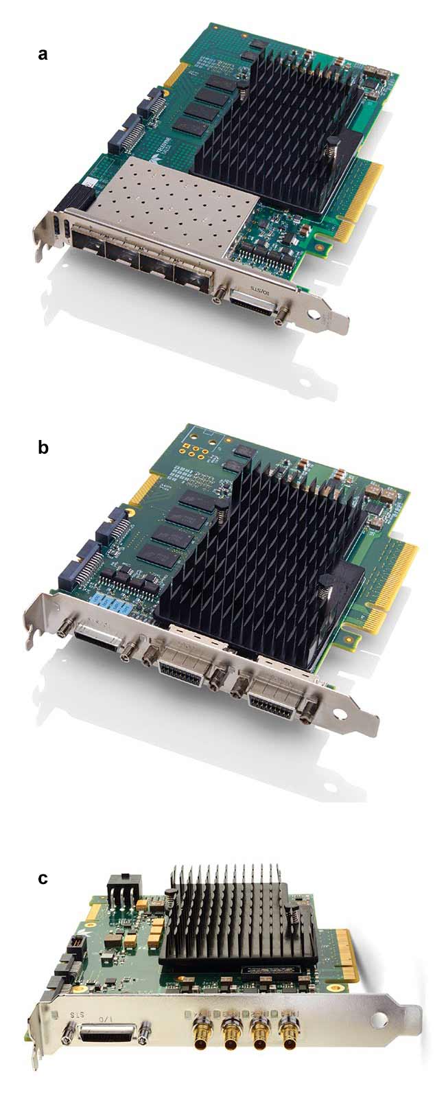
Figure 1. High-speed frame grabbers are available for CLHS,
supporting two levels of throughput with plug-in fiber cables (a, b), and for CXP over coaxial cable (c). Courtesy of Teledyne DALSA.
Optimization compromises
The balance between price, resolution, and speed has inspired creative solutions that deliver a compelling combination of features for specific industries. With their new Emerald sensors, Teledyne e2v has found a sweet spot for high resolution and low cost. The sensors achieve this with smaller pixels — 2.8 µm, the smallest global shutter pixels on the machine vision market. While still bigger than the 1- to 1.5-µm pixel size found in battery-constrained mobile phone cameras, the Emerald sensors are significantly smaller than the 5- to 6-µm-pixel sensors that were previously typical in machine vision applications.
The solution comes with compromises. At high speeds, light becomes scarce, and smaller pixels mean more noise in proportion to the amount of light falling on the sensor. However, if cost is the key driver, getting extra megapixels from a small camera can mean the difference between market success and failure. At the same time, the dropping cost-per-watt of LED lighting means illumination can also keep up with the increased demands on CMOS imagers.
These considerations are typical in applications such as food sorting, where bad products need to be grouped and removed from high-speed material streams. An individual grain of rice, for example, needs to be recognized as rice on a 3-m-wide conveyer moving at 5 m/s. This requires low-noise, high-resolution, and high-speed imaging all at the same time. It may take processing a lot of rice to justify upgrading a vision system, but applications such as traffic monitoring and logistics have shown that the return on investment with better systems can pay off immediately.
The parts of the system that receive the image have also become faster at receiving and processing the signal. Field-programmable gate arrays (FPGAs) have improved by leaps and bounds. Cabling options have improved as well. For instance, one of Teledyne’s frame grabbers with CXP-12 standard increases the capacity of each connection to 12.5 Gb/s, doubling the existing standard maximum data transfer rate support to 1.2 GB/s.
One cable alone can handle a 10-bit, 12-MP camera capturing more than
75 images/s. Up to four can be used concurrently. However, there are limits to what can be done over copper wires. CLHS (Camera Link HS, an AIA machine vision standard interface used by Teledyne), combined with optical cabling, can go even faster, handling seven-lane operations at 10 Gb/s using the interface’s X protocol in a single cable. This delivers host-transfer bandwidth of up to 8.4 GB/s. Even though computers continue to get faster, data rates such as these mean
camera data needs to (and can) be distributed for processing in parallel over multiple PCs.
Time delay integration
Because CMOS technology is so ubiquitous and performance keeps improving, it has become the starting point for applications that once seemed impossible. By integrating charge-domain TDI (time delay integration) pixels on a CMOS process, companies such as IMEC, Vieworks, and Teledyne Imaging have been developing sensor technologies that combine the best of both worlds.
TDI (Figure 2), a method of line-scanning that provides dramatically increased responsivity, has always been dedicated to high-end, low-light, high-performance applications. But as it’s been introduced to the world of CMOS, its approach to solving problems has expanded down, up, and out.
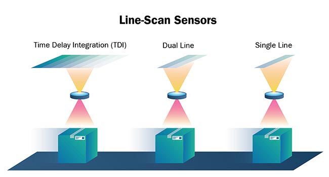
Figure 2. TDI (time delay integration), a method of line-scanning that provides dramatically increased responsivity compared to other video scanning methods, is based on the concept of accumulating multiple exposures of the same (moving) object. This effectively increases the integration time available to collect incident light, making it ideal for high-speed, low-light
applications. Courtesy of Teledyne DALSA.
Lately, sensor designers have begun to modify CMOS processes to allow for CCD-like pixels in which signal charge can be transferred from pixel to pixel. This allows the implementation of charge-domain TDI devices in which signal charge from multiple line integrations is summed without a corresponding increase in read noise. As illustrated in Figure 3, this allows for an increase
in signal-to-noise ratio (SNR) in proportion to the number of TDI stages. By implementing such functionality in a CMOS process, the SNR advantage of TDI technology can be combined with the simplified system integration potential, lower power, and faster readout of CMOS.
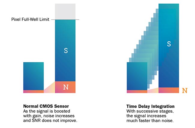
Figure 3. TDI functionality implemented in the charge domain allows for the scaling of signal in proportion to the number of TDI stages without a corresponding increase in read noise. This allows for much higher signal-to-noise figures than can be achieved with single-row line-scan imaging.
This has directly affected industries that experience challenges in both detail and scale, such as DNA sequencing. One of the most common methods of mapping DNA is to fluorescently label each of the four nucleotide bases of a DNA strand that represents the data of our genome. Since each base pair is about 0.5 nm across, the light from their fluorescence is extremely weak. High-sensitivity sensors are needed, and TDI is perfect. DNA analysis and sequencing can be used for the observation, identification, and characterization of biological systems, helping with pathogen and biohazard detection, disease screening, cancer diagnostics, and genetic research.
The new dimension of 3D
While TDI is a resolutely 2D approach, the power and speed of today’s CMOS sensors have driven imaging to a new dimension: 3D. There are several ways to perform 3D imaging, all of which have their own advantages and disadvantages.
1. Stereovision. This is the most common approach and it works similar to how our eyes work. Two cameras at different points are trained on the same object, with their feeds combined into a single 3D image.
2. Laser triangulation and structured light (Figure 4). In laser triangulation solutions, a single-line laser is partnered with an area-scan camera. The camera observes how the laser light deviates as it hits the object, providing a 3D map of the object. In structured light applications, multiple laser lines can be used for greater detail. (This is the same technology found in video game systems that can track movement.)
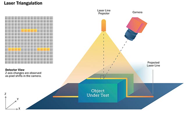
Figure 4. Laser triangulation: The distortion of a projected laser line is used to derive the dimensions of the object under test.
Courtesy of Teledyne DALSA.
3. Time-of-flight imaging. This works on the same principles as lidar, measuring the transit time of light between two objects in the scene. This technique is better for objects at greater distances.
While time-of-flight is used in automotive inspection, it tends to max out at the centimeter level, so it is less useful for precise robotics or machine vision applications. In contrast, the two methods mentioned above offer much better depth and detail up close, and can be accurate down to a matter of microns, recommending these two methods for applications such as metrology.
In all cases, the vision system tends to generate enormous amounts of data, with the amount of detail and speed being limited only by what the system can handle. With a well-tuned vision system, the smallest details make all the difference — fine defects in a crankshaft, imperfections in microscopic solder paste, or nuances in the surface inside a turbine.
Since CMOS is such a central technology for both consumer and industrial imaging, innovations from other corners of the silicon world keep finding their way into CMOS imaging. Just as Intel has announced not only memory and SoC (system on chip) stacking but also stacking of complex logic dies, companies are looking at ways to modify 3D sensor designs to achieve interconnects that are faster and more compact. By literally stacking memory, CPUs, and other key components under the camera, data has a very short distance to travel, which enables faster transfer.
Engineers are also finding ways to bring multispectral, hyperspectral, and polarized imaging to CMOS. The processes for making CMOS image sensors have been fine-tuned to make photosites sensitive far into the IR and UV ranges.
This new speed and cost-effectiveness of imaging sensors is yielding returns in other areas, including sorting different types of plastics for recycling. At the more extreme end of hyperspectral imaging, where hundreds of bands are tuned to specific wavelengths, scientists are able to detect the signatures of E. coli (Figure 5), contaminants, or food that has spoiled. Just as CCD-like pixels have found their way into CMOS sensors, engineers are bringing new materials to CMOS photosites — materials such as indium gallium arsenide (InGaAs) — to push spectral reception further beyond the sensing capabilities of silicon.
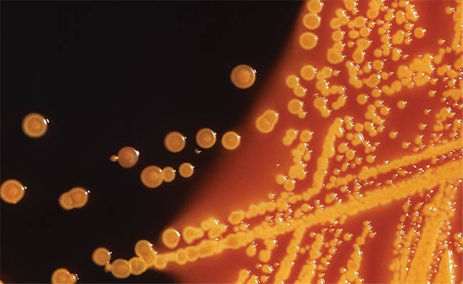
Figure 5. Colonies of Escherichia coli (E. coli) bacteria grown on a Hektoen enteric (HE) agar plate medium, as captured via hyperspectral imaging. Such colonies grown on HE agar display a characteristic, raised morphology, and are yellow to orange-yellow in color. Courtesy of the Centers for Disease Control and Prevention.
Feedback loop
Consumer needs are now driving CMOS technology in directions that benefit machine vision applications. In the future, machine vision is likely to be the driver of advancements that will benefit consumers. The average consumer is starting to have imaging and processing needs that rival those of industrial applications only a few years ago. A person may have thousands of photos on their phone, and the multicore CPU inside may be cranking away at an algorithm for facial recognition that started in a research lab somewhere. 3D imaging technologies that started in metrology and robotics are finding their way into video games and self-driving cars. IR imagers can even be paired with a smartphone to reveal gaps in home insulation.
Consumer applications may start looking a lot more like machine vision applications going forward. Image recognition, detection, and measurement may become killer apps for phones, appliances, and the Internet of Things. In the end, every industry will benefit from such applications. Machine vision systems will become faster and smarter, while consumer applications will become more innovative and seamlessly integrated into our daily lives.
Meet the author
Eric Fox, Ph.D., is director of CMOS image sensor R&D at Teledyne DALSA. His more than 25 years in the field have included development of image sensors, ranging from CCD technology to CMOS. He has bachelor’s and master’s degrees from the University of Toronto, where he also received his Ph.D. in physics (quantum optics); email: [email protected].
/Buyers_Guide/Teledyne_DALSA_Machine_Vision_OEM_Components/c3374