Elena Beletkaia, European Photonics Industry Consortium (EPIC)
Low-light cameras are designed with enhanced capabilities for recording images in settings with little to no illumination. These cameras perform well in poor lighting, in the dark, or with night vision. The fundamental components of a low-light camera are similar to those of a conventional camera, including lens, sensor, image processor, and optional additional IR cut filter. The two main types of sensors used in low-light cameras are CCD and CMOS sensors, which are both based on metal oxide semiconductor technology. However, CMOS sensors are less expensive to manufacture, and most producers have shifted to CMOS technology to offer more flexibility in the way pixels are read and processed. In-pixel architectures — such as the four-transistor (4T) structure, which achieves a higher conversion rate — and improvements to CMOS technology have greatly reduced the noise that CMOS sensors have historically produced.
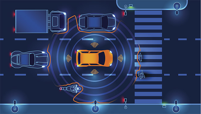
Sensors in an autonomous car scan the road. Courtesy of iStock.com/Andrey Suslov.
These changes have resulted in an industry-wide shift from CCD to CMOS sensors in recent years, enabling new applications in areas such as security and surveillance, driver assistance in automotive, space imaging, and low-light microscopy and photography.
Taking pictures at night usually results in a noisy or blurry image. The noise and blur are caused by the fact that almost all digital cameras have only red, green, and blue color pixels. These RGB cameras cannot reach optimal performance under low-light conditions because their optimal sensitivity is limited to the visible range. Low-light imaging conditions are defined as ambient light conditions under 1 lux of light flux, which is roughly comparable to the illumination of Earth’s surface during a full moon.
Photography is only one application of low-light imaging. Low-light cameras are also widely used in medicine and science — for example, for endoscopy imaging and continuous cell imaging. They are used for surveillance and monitoring at airports, banks, stores, and military installations. The growing demand for low-light imaging and sensing technologies is also being driven by advanced driver assistance systems in the automotive industry.
While the components of the low-light camera are similar to those of a conventional camera, low-light camera elements require enhanced capabilities for low-illumination conditions. The detector must have a large numerical aperture, high quantum efficiency, and signal amplification that can detect as many photons as possible emitted by the object. These properties, combined with a low readout noise, ensure a high signal-to-noise ratio. Furthermore, users from all industries are looking for high resolution, high dynamic range, high repetition rate, and low maintenance. Currently, there are four main camera technologies: CCD, CMOS, intensified, and electron multiplier. Of these, CCD and CMOS cameras hold the largest market share.
CCD cameras are based on traditional technology, and for a long time they were the only option available. Their high quantum efficiency and low read noise provide good sensitivity in near-IR illumination conditions. CCD technology continues to offer lower dark current than CMOS. But because of the serialized structure of CCD imagers, they are slower than CMOS imagers, which can read out a great deal of data simultaneously. Therefore, CMOS technology is preferred for high-speed imaging. However, low-light, high-speed imaging has been problematic for CMOS technology because the global shutter CMOS devices that are used in high-speed imaging are much noisier than the rolling shutter devices usually used for low-light cameras, and they are even noisier than some CCDs. This is due to the more complex architectures of global shutter devices, which require more transistors in their pixel sensors. Sensor manufacturers are taking notice. First Light Imaging released the first low-noise, high-speed global shutter architecture scientific CMOS camera last year. The company’s C-BLUE One camera was developed for astronomical laser-assisted adaptive optics (Figure 1).
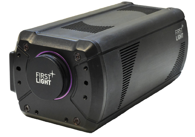
Figure 1. The C-BLUE One scientific camera has a 1608 × 1104 monochrome CMOS sensor and a 660-fps global shutter. Courtesy of First Light Imaging.
Dynamic range can be a critical parameter in sensors, such as those that provide driver assistance in automobiles. Huge contrast between very bright objects, such as headlights, and very dark items, such as road obstacles, must be managed within one image. In autonomous vehicles, image sensors must be able to distinguish between a car, a truck, a bike, and a scooter based on recognizing headlight separation (recognizing the number of headlights and the distance between them, for example). While CCDs have a good dynamic range, CMOS sensors have more transistors per pixel. This means that CMOS sensors have an increased well capacity or total charge that each pixel can hold during integration, leading to even higher dynamic range.
CCD technology can also produce blooming and smear, which can result in vertical lines in the image when a bright spot is in the field of view, obstructing the data interpretation and impeding overall performance. CMOS technology is resistant to blooming and smear. However, it can produce other image artifacts. The total noise level of a CMOS sensor is typically greater than that of a CCD sensor, and this difference increases with higher temperatures. A potential solution currently being researched is upconverting an IR image to visible wavelengths. Such upconversion can be realized via nonlinear wave-mixing of shortwave IR images, using a strong near-IR pump beam within a resonant ultrathin GaAs metasurface. Such an all-optical approach is not affected by thermal noise and can operate at room temperature using conventional CMOS detectors.
Further improvements in CMOS technology have enabled the development of custom CMOS image sensors for the most demanding functions, including photon-starved applications such as imaging the cosmos or within the human body, where it is important to be able to detect every pixel for analysis. Companies such as IMASENIC have developed conventional active pixel CMOS sensors that achieve noise performance at the single-electron level (Figure 2).
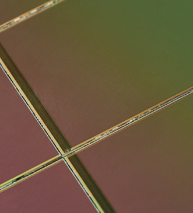
Figure 2. A low-noise 2-MP sensor on its wafer. Courtesy of IMASENIC.
With avalanche diodes integrated into sensors, not only can individual photons be detected, but their arrival times can be precisely determined. This enables depth measurements through time-of-flight determination. IMASENIC integrated sensing with signal conditioning, including the analog-to-digital conversion. And all the controls are easily accessible through a digital interface. Thus, a single chip basically performs all the functions of a camera. IMASENIC’s innovations have helped CMOS sensors reach efficient detection in the NIR to SWIR (on the long-wavelength side of the spectrum), in the UV, and even for low-energy x-rays (for shorter wavelengths).
Clearly, CMOS technology is dominating the low-light imager market due to the advantages CMOS sensors offer over CCD sensors, including small size, low power consumption, easy integration, faster frame rate, and lower manufacturing cost.
Meet the author
Elena Beletkaia, Ph.D., is project leader at the European Photonics Industry Consortium (EPIC). Within EPIC, she is responsible for sensing technologies and life science applications. Her background includes a degree in biophysics from Lomonosov Moscow State University and a doctorate from Leiden University, including extensive work on the biochemical and biophysical mechanisms of cancer metastasis and the application of multiple microscopic and spectroscopic techniques for sensing and noninvasive imaging; email: [email protected].