
Camera Selection for Low-Light Imaging
Providing excellent performance at reasonable prices, uncooled CMOS cameras offer a viable alternative to CCDs in low-light imaging applications.
FELIX ASCHE, BASLER AG
Fluorescence microscopy is a broadly used term, with applications ranging from basic life science, such as time-lapse cell viability assays, to sophisticated techniques in which a very few photons or single molecules are detected and localized by specific high-end hardware and software. It further extends to even more sensitive biochemistry detection methods that leverage, for example, chemiluminescence and bioluminescence.
Low-light imaging technology is instrumental to all of these microscopy applications, and often finds use in macroscopic optical systems. Although fluorescence microscopy technology is quite mature, camera selection for specific applications remains challenging. It can be complex to design a cost-effective optical imaging system that is optimized for a particular task, and end users can benefit from an overview of the major technical aspects that should be considered when choosing imaging components.
It is useful to know, for example, that overall system costs increase with the selection of larger optical formats, such as the F-mount. The most common mount is the C-mount, which, with up to 1.1-in. sensors, delivers very good optical performance at a reasonable price. The smaller S-mount is a good choice when minimizing size and cost are a priority. Squared sensors are often preferred in microscopy to capture the maximum image content.
Because the sensor assumes such a central role in an imaging system, understanding certain performance specifications is of major importance.
Sensor taxonomy
Since the late 1970s, CCD sensor technology has been well established and is still available in high-end microscopy cameras. Sony, the leading manufacturer of CCDs globally, has discontinued the technology, forcing instrument manufacturers to find alternative cameras for their systems. Meanwhile, newer CMOS technology has spread through consumer sensor markets and has recently become competitive. CMOS noise levels have achieved comparable or better performance than conventional CCDs, enabling the newer technology to deliver higher speed, higher resolution, and less power consumption and heat dissipation, at a lower price point for medical and life science applications.
Scientific CMOS (sCMOS) cameras were introduced in 2010 to further improve performance versus CCDs, mainly through faster readout speeds and higher dynamic range.
CMOS sensor development is still rapidly accelerating, offering innovations
such as backside illumination (BSI), which found its way into industrial image sensors, where it significantly improves the pixels’ quantum efficiency. Designed for the smartphone market, with its demand for smaller pixels, backside illumination reverses the orientation of the pixel structure to present the light-sensitive photodiode directly below the microlenses. With this design, the metal wiring structures no longer inhibit the incident photons, improving the so-called fill factor (the relation of the photoactive and nonphotoactive area) of the pixels (Figure 1).
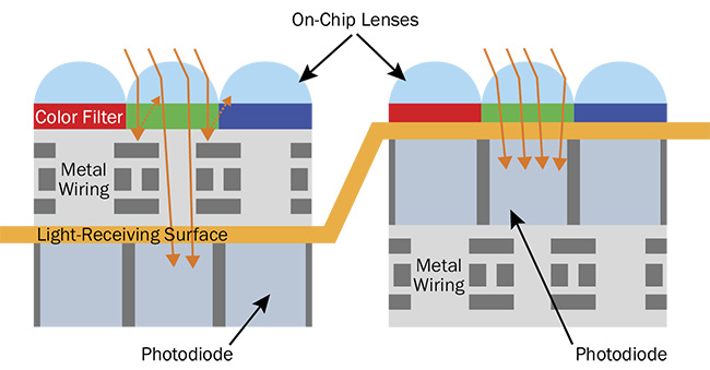
Figure 1. State-of-the-art frontside illuminated sensors (left) perform excellently in low-light conditions, but the design of backside-illuminated pixels (right) offers significantly improved quantum efficiency. Courtesy of Basler AG.
However, backside-illuminated sensors can have additional noise sources contributing to their dark current, or the leakage of electrons during exposure. This can make these sensors less than perfect for applications requiring long exposure times. State-of-the-art frontside-illuminated (FSI) sensors also show excellent performance in low-light conditions, and may still be a better choice in certain applications (Figure 2).
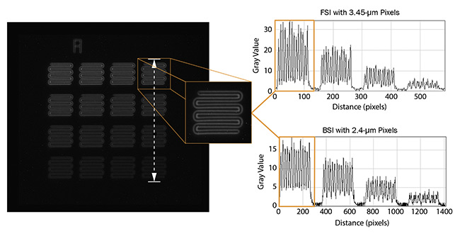
Figure 2. A persistent fluorescence carrier with 8.5-µm structures of varying intensity was imaged by two sensors — one backside-illuminated (BSI) and the other frontside-illuminated (FSI) — under the same microscope setup (the same optical path, lighting, and 10-s exposure time). For the FSI camera, the histogram shows nearly doubled gray values. Courtesy of Basler AG.
Two additional high-end sensor types include electron multiplying CCDs and intensified CCDs. Neither are as widely used as conventional CCDs or CMOS because the technology is expensive and targets mostly niche applications.
CMOS technology will continue to evolve and can be expected to dominate low-light applications in the future.
Monochrome or color
For low-light applications, monochrome cameras are usually preferred because of their higher quantum efficiency versus color cameras. In color cameras, Bayer microfilters on each pixel let only certain wavelengths pass through, which means fewer photons reach the photon-reactive area of the pixel. In addition, the IR-cut filter in color cameras further blocks wavelengths from ~650 to 700 nm and upward (Figure 3).
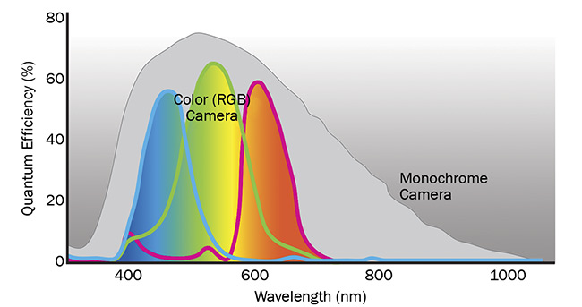
Figure 3. Because of the red, green, and blue color filters applied to the pixels of color cameras, the quantum efficiency of these devices is lower compared to monochrome cameras. In addition, color cameras typically come with an IR-cut filter blocking light from ~650 to 700 nm and upward. Courtesy of Basler AG.
Typically, images with multiple fluorescence markers for detection and co-localization of molecules of interest are made from separate images using monochrome cameras. Selectable light sources and filter sets provide the right combination of excitation and emission wavelengths for each fluorophore used (Figure 4).
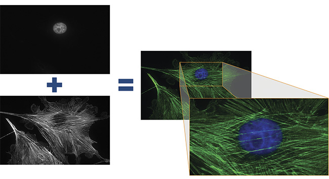
Figure 4. Two fluorescence images of a cell substrate were taken with a front-illuminated monochrome CMOS sensor in a 2.3-MP monochromatic camera. The exposure times were 500 ms at 63× magnification. The two images on the left, showing the cell nucleus (top) and filamentous actin (bottom), were colored by software and merged to show both structures in one image (right). Courtesy of Basler AG.
However, certain applications may create a demand to use only one camera for color imaging and fluorescence. This is possible if the sensitivity demands of the fluorescence application are not too high.
Global and rolling shutters
CCD sensors have only one shutter type (global), while CMOS sensors offer two: rolling and global. Shutter type has a significant impact on image quality, especially when target objects are moving. In rolling shutter sensors, the pixels are exposed line after line. As a result, an object that has changed position between the signal capture of two lines can cause space distortion in the image. The advantage of rolling shutter sensors is that they have fewer electronic parts in the pixel, which can result in less noise during readout. Conversely, global shutter sensors expose all pixels at the same time. There is no time shift between the exposures of the various pixel lines, and consequently no space distortions when imaging moving objects.
Imaging systems for low-light micros-copy clearly need to be sensitive enough to capture very faint light signals. Sensitivity should be understood as the minimum amount of light required to generate a signal that can be distinguished from noise. One important metric for this is quantum efficiency (QE), which describes the ratio between the incident photons of the light source and the generated electrons of the pixel.
Quantum efficiency depends on wave-length, and the spectrum of a given sensor should correspond to the emission spectra of the fluorophores in the application. Higher quantum efficiencies enable shorter exposure times, and thereby reduce photobleaching of fluorophores and shorten scanning time.
Often, it is beneficial to resolve a wide range of light intensities with one exposure. Here, the full-well capacity of a sensor becomes relevant. It describes the maximum number of electrons that can
be generated by one pixel per exposure.
A higher full-well capacity permits capture of more light before a pixel is saturated, potentially reducing the need for additional exposures.
A sensor’s dynamic range combines its full-well capacity with its read noise (the lowest number of electrons required to produce a true signal) to characterize a camera’s overall ability to measure and distinguish various levels of light. Additionally, there is the absolute sensitivity threshold, which is the number of photons required by one pixel to generate a signal-to-noise ratio of 1, meaning the signal is equivalent to the noise. The smaller this value, the less light a sensor requires to produce a true signal. Because absolute sensitivity threshold does not take pixel size into account, it cannot directly help when comparing two cameras with different pixel sizes.
Depending on the quantification requirements of the application and the technical dynamic range of a given camera, the bit depth of the pixel determines the number of gray values that can be differentiated.
Typical machine vision cameras have a depth of 8 bits (28 or 256 gray values), which is sufficient for visual needs, since the human eye can resolve only 6 to 7 bits. Beyond that, 12 bits (212 or 4096 gray values) is common and technically adequate for the majority of cases. However, certain scientific applications demand 14 or even 16 bits (214/216 or 16,384/65,536 gray values). Image file sizes significantly increase with bit depth, potentially affecting processing and data storage, as well as interface bandwidth.
Image quality and noise
Noise is the deviation between the true signal value and the value produced by a measuring system. The signal-to-noise ratio (SNR) quantifies the overall noise of an imaging system at a certain light level and is a common parameter used to compare cameras. The higher the signal-to-noise ratio, the better the image quality. In the imaging process, certain types of noise can rarely if ever be reduced by the camera technology (for example, photon/shot noise). However, other noise types that influence image quality are significantly affected by the sensor itself and the camera technology. Read noise — or temporal dark noise — is added to a signal per one shutter event and is defined as
e−/pixel. Modern CMOS sensors go down to a read noise of only 2 e−/pixel (Figure 5).
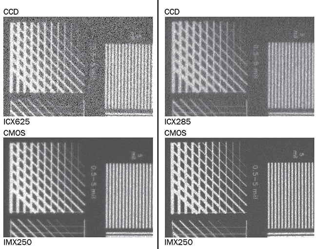
Figure 5. A comparison of the temporal dark noise behavior of CCD and CMOS cameras, with an exposure time of 10 ms. Temporal dark noise — or read noise — is added to an imaging sensor’s signal per one shutter event. Courtesy of Basler AG.
Another noise source that becomes increasingly relevant for low-light applications as exposure times increase is caused by dark current, which is expressed as e−/pixel/s (Figure 6). As a rule of thumb, dark current doubles with each temperature increase of 7 °C.
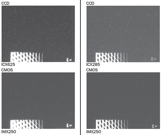
Figure 6. A comparison of dark current noise behavior in CCD and CMOS cameras with an exposure time of 4 s. The noise from dark current in imaging sensors increases with exposure time, as well as temperature. As a rule of thumb, dark current doubles with each temperature increase of 7 °C. Courtesy of Basler AG.
Noise types that describe not a temporal- but a space-related behavior are called fixed-pattern noise, which describes deviations that can be seen between various pixels. It can be caused by the pixel electronics or by inconsistent temperatures over the sensor area. Standardized quantification measures of these noise types include dark signal nonuniformity (DSNU), which describes the deviation of generated electrons without any light signal, and photoresponse nonuniformity (PRNU), which describes the pixel-to-pixel deviation at a certain light level. By setting cutoff values on pixel-to-pixel deviations, one can further differentiate and describe outlying pixels as defect pixels — such as hot pixels — that show high gray values without a corresponding signal. Certain camera manufacturers already correct defect pixels during quality control by interpolation of neighboring pixels so integrators are not impaired by these artifacts.
Image preprocessing
There will never be a perfect camera that provides an ideal image, which is why an image must undergo a series of preprocessing steps to refine the raw image into one with more fidelity to the imaged object. The biggest challenges that arise from long exposure times are spatial inhomogeneities, hot pixels, and noise caused by dark current.
One approach to eliminating spatial
inhomogeneities is dark-frame subtraction, wherein a dark image is taken in a given setting and is afterward subtracted from images with respective objects or content. This results in a clear image showing only the signals arising from the object (Figures 7 and 8). The disadvantage of this method is that it is valid only at the operating point at which the dark frame was taken, which makes it less flexible to changes in the application.
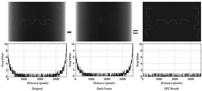
Figure 7. Dark-frame subtraction can eliminate spatial inhomogeneities in an image. Visibility of weak object structures within brighter sensor areas is poor
(right and left vertical lines in original image) (left). After subtraction of the dark frame, the image background is homogeneous (see also respective histogram),
resulting in better visibility of image content (right). Courtesy of Basler AG.
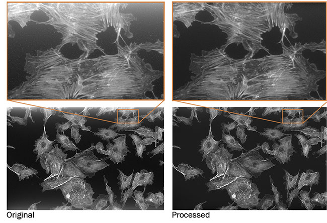
Figure 8. To demonstrate dynamic correction of spatial inhomogeneity and defect pixels, a cell substrate was imaged on a fluorescence microscope using a monochrome CMOS camera. Exposure time was 5 min at 20× magnification (left). A dark and homogenous background and nearly no defect pixels appear in the processed images (right). Courtesy of Basler AG.
Some sensors provide optical black pixels that can be used to recalculate the signals of normal pixels to improve image quality at long exposure times. This is similar to dark-frame subtraction, but it can be done dynamically — without the need to use pre-captured dark frames — and is thereby not restricted to given operation points.
Hot pixels are typically clearly visible and become even more evident at longer exposure times, for which static integrated correction by the manufacturer may not be sufficient. The solution is dynamic defect pixel correction, in which intelligent algorithms identify deviating pixels and calculate correct gray values based on the surrounding pixels.
Spatial denoising approaches are not applicable to reducing temporal noise. Instead, other methods such as median filters can be used. Artificial intelligence and deep learning methods are also introducing new ways to improve the possible performance of current temporal noise reduction, while preserving the finer structures of image content (Figure 9). It should be noted that image processing can typically run on a camera’s field-programmable gate array or host PC. Integration of the function in the camera’s field-programmable gate array produces faster results and reduces performance-related costs caused by host system requirements.
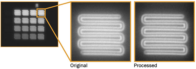
Figure 9. AI and deep learning software are introducing new ways to reduce temporal noise in images. A persistent fluorescence carrier with small, 8.5-µm structures of varying intensity was imaged on a microscope. Exposure time: 1 s; gain: 24 dB 2×2 average binning; 40× magnification (left and center). Temporal noise is reduced by AI-based image processing (right). Courtesy of Basler AG.
Cooling
The temperature of the sensor has a central impact on dark current, which decreases the signal-to-noise ratio and image quality — especially when light signals are weak and longer exposure times are required. Cooling of cameras is therefore an important if not necessarily mandatory consideration in low-light imaging.
Because active cooling measures such as Peltier cooling significantly affect a camera’s total cost of ownership, the majority of imagers are not actively cooled. This is acceptable for applications with sufficient signal strength. However, heat production should be avoided by designing the imaging operation for low power consumption, and heat should be efficiently dissipated both by the camera’s hardware design (by the camera manufacturer) to provide an efficient passive cooling, and by mounting the camera to a further heat-dissipating carrier (by the camera integrator).
Combining modern CMOS sensors with effective passive cooling and state-of-the-art image processing strongly expands potential exposure times from several seconds to many minutes to provide excellent image quality that is comparable to or better than that of actively cooled CCD cameras.
Signs point to CMOS
The current generation of CMOS sensors enables low-light imaging applications that were formerly impossible without a significant investment in cooled CCD camera technology. These new possibilities are particularly relevant as fluorescence- and luminescence-based imaging methods become increasingly applied in the life sciences, in medical or in vitro diagnostics, and for capturing molecular processes and target structures, such as pathogenic viruses.
Further, with Sony’s discontinuation of its CCD product group, manufacturers in the medical and life sciences need to find an alternative imaging technology to integrate into their instruments. Providing a compact form factor and excellent performance at reasonable prices, uncooled cameras with CMOS sensors can be the right choice for them.
Meet the author
Felix Asche, Ph.D., is product market manager for Basler AG. Before joining Basler in 2016, he was a product manager in the area of automation for a leading
global manufacturer of medical lab
diagnostics.
/Buyers_Guide/Basler_AG/c1527