Tony Chapman, Thermo Fisher Scientific
An industry expert offers a primer on the advantages of charge-transfer-device imagers.
In imaging devices, radiation normally affects certain key parameters – gate threshold voltage, field/channel stop threshold voltage, charge transfer efficiency, dark current and noise – but a charge-injection-device (CID) imager can overcome these radiation effects.
A CID is a broadband (200 to 1100 nm) charge-transfer-device (CTD) image sensor with capabilities very different from those of typical commercially available charge-coupled devices (CCDs), CMOS and active pixel sensors. CTDs, including the CID imager, use hundreds of thousands – up to 4 million – pixel elements to capture optical images and convert the light into an electronic charge that can be displayed on a monitor or captured and processed by a computer.
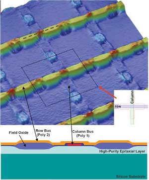
A CID is a broadband (200 to 1100 nm) charge-transfer-device image sensor that uses hundreds of thousands of pixel elements – up to 4 million – to capture optical images and convert the light into an electronic charge. Here, the structure of a CID image sensor.
The CID imager differs from other CTDs in that its architecture can be configured as a radiation-hardened device that operates reliably in a wide range of radiation environments beyond the typical lifetime of CCD- or CMOS-based cameras – in some cases, by orders of magnitude.
The CID also can be configured as a random-access CID device capable of randomly addressing individual pixels and interrogating pixel charge nondestructively for higher signal quality and extended linear dynamic range for scientific imaging applications.
Gate threshold voltage
Ionizing radiation causes positive charge to accumulate in the MOS (metal-oxide semiconductor) transistor gate oxide, which reduces the gate and field voltage thresholds in N-channel transistors. Also, the drain-source standoff voltage decreases as radiation exposure increases. If the accumulated radiation is sufficiently high, the transistor will turn on permanently and cease to function as a switch. This type of device will short out. Conversely, when P-channel transistors are exposed to radiation, the threshold voltage (Vth) becomes more negative; therefore, a more negative voltage is required to turn on the transistor. This shortcoming of the P-channel transistor allows it to be controlled as an “on” or “off” switch.
Typical commercially available CCD imagers are fabricated using N-channel technology; consequently, exposure to radiation causes the CCD register photogates to “turn on” into one continuous channel, and the devices short out. This catastrophic failure may occur in as little
as 10- to 20-krads total ionized dose to gamma (60Co) exposure.
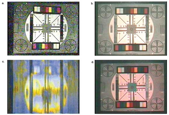
When commercially available CCD imagers are exposed to radiation, the CCD register photogates “turn on” into one continuous channel, and the devices short out. This can occur with total-dose gamma (60Co) exposure as low as 10 to 20 krads. Here, images from a commercial CCD camera and the standard CID8825DX6 camera when exposed to a gamma source (60Co): a and b show the CCD and charge-injection-device (CID) imagers, respectively, with no radiation exposure. Image c shows deterioration in the CCD image after just 1 h of radiation exposure, but the CID image in d is much less affected after 45 h of exposure.
Radiation-hardened CIDs are fabricated using P-channel technology and will continue to function in radiation environments. Pixel and logic operation is extended well into the megarad range by sensing the Vth shifts that occur on the device and dynamically adjusting the image sensor drive voltages to compensate for the resulting shift in gate threshold. The CID design, speed of operation and choice of process determine the limits of operation.
Channel stop threshold voltage
The positive charge that accumulates because of ionizing radiation in the field oxide regions that isolate MOS transistors causes a channel to form and to couple unrelated N-channel transistors and photo-pixel structures; this makes them short out in as little as 10 to 20 krads total-dose gamma (60Co).
But, conversely, the isolation present in the P-channel CID radiation-hardened devices improves between unrelated transistors and photo-pixels, and the CID will continue to function in significant radiation levels to a minimum of 3 Mrads, or
3 x 10⁶ rads total-dose gamma (60Co).
Charge transfer efficiency
Incomplete lattice bonds are formed at the surface of the silicon substrate because of the lack of silicon neighbor atoms. These bonds are usually completed using a hydrogen-annealing process. High-energy radiation can easily displace silicon atoms, disrupt the hydrogen-annealed bonds, and the bond locations become “traps” for photon-generated charge. These surface traps also degrade devices’ temporal noise and thermally generated dark current.
For the case of a large-surface channel CCD that might require 1000 charge transfers through a charge-coupled shift register, a transfer efficiency of 99.5 percent would result in 0.7 percent of the final signal charge read out at the output preamplifier. For a similar “buried channel” CCD, a charge transfer efficiency of 99.9995 percent would result in 99.5 percent of the final signal charge read
out at the output preamplifier. Because of this issue, any charge transfer problem of a CCD is circumvented through the use of a buried channel. However, exposure to ionizing radiation significantly increases the trap density in the buried channel CCD device, which, in turn, lowers charge transfer efficiency, causing the visible scintillation noise most commonly seen with CCDs.
Similar to a CCD, the CID sensor also experiences degradation of charge transfer efficiency when exposed to radiation. However, unlike the CCD structure, the reduced charge transfer efficiency has minimal impact on the performance of the CID sensor. The charge readout is achieved using a single charge transfer occurring within the individual CID pixel structure itself, so the pixel charge is not shared with entire rows or columns as it is with CCDs. Therefore, charge transfer efficiency is typically not an issue with CID devices until significantly higher damaging radiation flux rates.
Noise
A function of trap density, 1/f noise increases dramatically with ionizing radiation and higher temperature. Optimizing the silicon process helps to minimize the generation of charge traps in the CIDs. Using the advantages of correlated double sampling also can help reduce the effect of low-frequency 1/f noise.
In CIDs, gamma- and neutron-impact-induced noise is minimized by reducing the thickness of the “active” layer; however, in high-radiation flux rates (.100 krads/h), some scintillation or random noise in the image may be observed on Thermo Fisher Scientific’s MegaRAD series imagers that may not be present in the passive-pixel version radiation-hardened CID imagers. This series of cameras exhibits higher light sensitivity and higher total-dose capabilities. The significantly increased light sensitivity means that the primary noise exhibited in these devices is the result of individual ionizing energy loss (IEL) radiation events striking and being detected within the associated pixel sites.
Dark current
Dark current, which is also a function of trap density, increases dramatically with radiation and higher operating temperature. Lowering the operating temperature by using a Peltier, or thermoelectric, cooler and optimizing the silicon process can help minimize the dark current.
Total-dose tolerance
The camera is designed to compensate for the Vth shifts in the image sensor. This is achieved by driving the imager circuitry at biases as determined by an empirically generated algorithm. Nonionizing energy loss (NIEL) can lead to bulk damage such as displacement of silicon atoms in the silicon; NIEL-induced damage introduces permanent defects that are the primary cause of elevated dark current and poor charge transfer efficiency after exposure to radiation. A thermoelectric cooler can compensate for the increased dark current resulting from NIEL to maintain operating temperature at 25 °C, even at elevated ambient temperatures up to 50 °C.
Total-dose-radiation tolerance is dependent upon numerous factors, including but not limited to duty cycle; type of radiation (gamma ray, x-ray, neutron); typical dose rate; ambient temperature; and, by some accounts, silicon wafer-to-wafer process variations.
Duty cycle is among the most important factors. The extent and severity of radiation damage is much greater when the camera is under power than when it is powered down. Therefore; a camera powered and operated for only brief intervals on a daily or weekly basis will have a longer lifetime in radiation environments than one operated continuously.
Based upon the typical MegaRAD imager Vth shifts and the bias/drive voltage adjustment range, with 100 percent duty cycle – i.e., with the camera always powered and running – as tested with a 60Co (gamma) source, these cameras will continue to function to at least a total-dose exposure of 3 x 10⁶ rads (total-dose gamma). The cameras, available with either monochrome or color output, exhibit sensitivity and noise performance on par with typical commercial CCD/CMOS cameras.
Meet the author
Tony Chapman is sales and marketing director of CIDTEC cameras and imagers in the Chemical Analysis Div. at Thermo Fisher Scientific
in Liverpool, N.Y.; email: [email protected].
For more information
on charge-injection devices, see Tony Chapman’s article on detectors in the Photonics Handbook, viewable online at https://www.photonics.com/a25130.