A research team led by professor Ming Wu at the University of California, Berkeley is developing a high-resolution, chip-based lidar system that could be used in a range of devices, from autonomous cars to smartphones. The researchers used a focal plane switch array (FPSA) with MEMS switches to pack 16,384 pixels on a 1-sq-cm chip.
FPSA-based 3D sensors for solid-state lidar systems can support electronic scanning without requiring unwieldy mechanical moving parts.
So far, however, the resolution of these sensors has been limited to 512 pixels.
Mechanical lidar systems have powerful lasers that can visualize objects hundreds of yards away and generate high-resolution 3D maps. Putting the capabilities of these lasers on a chip has challenged researchers for more than a decade.
“We want to illuminate a very large area, but if we try to do that, the light becomes too weak to reach a sufficient distance,” Wu said. “So, as a design trade-off to maintain light intensity, we reduce the areas that we illuminate with our laser light.”
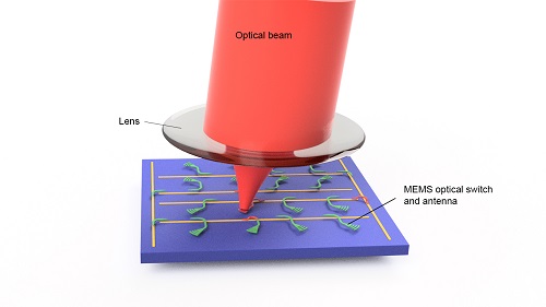
A schematic of a lidar chip. Laser light is emitted from an optical antenna connected to a tiny switch. Reflected light is captured by the same antenna, and 3D images are obtained by sequentially turning on the switches in the array. Engineers at the University of California, Berkeley used MEMS switches to significantly increase the resolution of chip-based lidar sensors. Courtesy of Xiaosheng Zhang/UC Berkeley.
FPSAs use a camera-like optical system that maps each angle within the field of view to a pixel at the back focal plane of an imaging lens. Instead of integrating a ranging unit at each pixel, the optical switch network in the FPSA allows all pixels to share one or more ranging units. Each pixel consists of only one optical antenna and a switch, enabling a large array to be integrated on a single chip. All available laser power can be channeled through one antenna at a time.
Silicon-based lidar systems typically use thermo-optic switches to redirect laser light from one waveguide to another. The UC Berkeley team chose to use MEMS switches to physically move the waveguides in the lidar system from one position to another.
“The construction is very similar to a freeway exchange,” Wu said. “Imagine you are a beam of light going from east to west. We can mechanically lower a ramp that will suddenly turn you 90°, so that you are going from north to south.”
In addition to being smaller and more energy-efficient than thermoelectric switches, MEMS switches are faster and exhibit low light losses. These advantages have been demonstrated in large-scale optical switches for optical communications networks. The researchers said, to the best of their knowledge, their team is the first to use MEMS switches for lidar.
The team integrated a 128- × 128-element FPSA of grating antennas and MEMS-actuated optical switches on a 10- × 11-sq-mm silicon photonic chip. In experiments, the researchers achieved 3D imaging with a distance resolution of 1.7 cm by using frequency-modulated continuous-wave (FMCW) ranging in a monostatic configuration.

With a 5-mm-focal-length compound lens, the system randomly directs the laser beam to 16,384 distinct directions in a 70° × 70° field of view, with a 0.05° divergence angle and a microsecond switching time. Each pixel is equivalent to 0.6° of the array’s 70° field of view. 3D imaging is realized by combining the FPSA with FMCW ranging. The FPSA's design is scalable to megapixel sizes by using the same CMOS technology that is used to produce computer processors.
By cycling rapidly through the array, the FPSA constructed a 3D image of its surroundings. Several FPSAs, arranged in a circular configuration, could provide a 360° view around a vehicle.
Before commercializing the system, Wu and his team plan to increase the resolution and range of the FPSA. “While the optical antennas are hard to make smaller, the switches are still the largest components, and we think we can make them a lot smaller,” Wu said.
The system’s range, which is currently 10 m, will also be increased. “We are certain we can get to 100 m and believe we could get to 300 m with continual improvement,” Wu said.
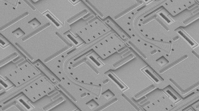
A scanning electron micrograph of the lidar chip showing the grating antennas. The researchers integrated a 128 - × 128-element focal plane switch array (FPSA) of grating antennas and MEMS-actuated optical switches on a 10- × 11-sq-mm silicon photonic chip. In experiments, the team achieved 3D imaging with a distance resolution of 1.7 cm by using frequency-modulated continuous-wave (FMCW) ranging in a monostatic configuration. Courtesy of Kyungmok Kwon/UC Berkeley.
With these enhancements — and with the ability to mass-produce the FPSA using conventional CMOS production technology — inexpensive, chip-size lidar could become ubiquitous, leading to a new generation of low-cost, energy-efficient 3D sensors for autonomous cars, drones, robots, and smartphones. In addition to 3D sensing applications, the FPSA could be used in applications that require optical beam steering, such as free-space optical communications and trapped-ion quantum computation.
“Just look at how we use cameras,” Wu said. “They’re embedded in vehicles, robots, vacuum cleaners, surveillance equipment, biometrics, and doors. There will be so many more potential applications once we shrink lidar to the size of a smartphone camera.”
Wu was recently named one of the participating researchers in Intel Labs’ newly opened Intel Research Center for Integrated Photonics for Data Center Interconnects. His project called “Wafer-scale optical packaging of silicon photonics” will lead to the development of integrated waveguide lenses that have the potential to enable noncontact optical packaging of fiber arrays with low loss and high tolerances.
The research was published in Nature (www.doi.org/10.1038/s41586-022-04415-8).