
Collaboration to Bring Nanoimprint Lithography to Mainstream Manufacturing
ST. FLORIAN, Austria, Sept. 27, 2022 — EV Group (EVG) — a provider of wafer bonding and lithography equipment for the MEMS, nanotechnology, and semiconductor markets — and photomask provider Toppan Photomask Co. Ltd. entered into an agreement to jointly market nanoimprint lithography (NIL) as a high-volume manufacturing process for the photonics industry. Together, the companies will provide NIL development kits that include master templates from Toppan Photomask and equipment and process development services provided by EVG.
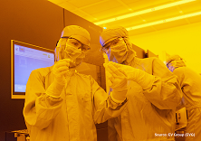
Process engineers examine a 200-mm wafer with metalenses replicated using a master manufactured by Toppan Photomask and a nanoimprint lithography process from EVG. The companies are collaborating to establish the process as an industry standard for photonics manufacturing. Courtesy of EV Group.
The collaboration aims to establish NIL as an industry standard production process for photonics manufacturing. EVG will offer NIL technology and product demonstrations at the NILPhotonics Competence Center at its headquarters in Austria.
The collaboration is nonexclusive.
/Buyers_Guide/EV_Group_EVG/c4622
/Buyers_Guide/Toppan_Photomasks_Inc/c16681
Published: September 2022
Glossary
- nanoimprint lithography
- Nanoimprint lithography (NIL) is a nanolithography technique used for fabricating nanoscale patterns on a substrate. It is a high-resolution, high-throughput process that involves the mechanical deformation of a resist material on a substrate to create the desired nanostructures. The process is similar to traditional embossing, where a mold or template is pressed into a material to replicate a pattern.
Here are the key elements and steps involved in nanoimprint lithography:
Template/mold...
- lithography
- Lithography is a key process used in microfabrication and semiconductor manufacturing to create intricate patterns on the surface of substrates, typically silicon wafers. It involves the transfer of a desired pattern onto a photosensitive material called a resist, which is coated onto the substrate. The resist is then selectively exposed to light or other radiation using a mask or reticle that contains the pattern of interest.
The lithography process can be broadly categorized into several...
- semiconductor
- A semiconductor is a type of material that has electrical conductivity between that of a conductor and an insulator. In other words, semiconductors have properties that are intermediate between metals (good conductors of electricity) and insulators (poor conductors of electricity). The conductivity of a semiconductor can be controlled and modified by factors such as temperature, impurities, or an applied electric field.
The most common semiconductors are crystalline solids, and they are...
- photomask
- A photomask, also known simply as a mask or reticle, is a key component in the photolithography process used in semiconductor manufacturing and other areas of microfabrication. It is a high-precision plate or glass substrate that carries a pattern of opaque and transparent regions. Photomasks are crucial for transferring intricate patterns onto semiconductor wafers during the photolithography process.
The photomask is typically placed in the optical path between a light source and a...
BusinessindustrycollaborationNILnanoimprintnanoimprint lithographylithographymanufacturingsemiconductorOptics ManufacturingMEMSphotomaskToppan PhotomasksEV GroupEurope