TOKYO, Dec. 22, 2021 — Pixel-scale metasurface lenses can be used to make imaging sensors roughly three times more sensitive than those currently in use, according to research from NTT Device Technology Labs. The sensor architecture introduced by the team could enable digital cameras that can image at higher speeds or in conditions with less light.
“Traditional imaging sensors such as the ones used in smartphones, wearable devices, and autonomous vehicles have a limited sensitivity because they rely on color filters placed over each pixel,” said research team leader Masashi Miyata from NTT Device Technology Labs in Japan. “Our new metalenses are made from a highly engineered surface that can collect light while simultaneously separating primary colors without any color filters, opening a pathway to dramatically improve sensitivity.”
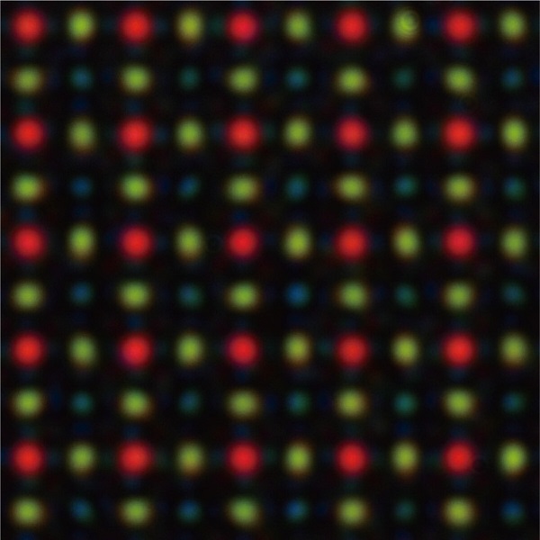
This color microscopy image shows the measured light profile on the sensor pixels under normal illumination. The efficiency of color sorting and focusing into each target pixel can be observed. Courtesy of Optica.
Miyata’s team reports that filter-free color sensors made with its metalenses significantly enhanced signal levels without sacrificing color image quality or spatial resolution. Because the metalenses are made using a CMOS-compatible process, they could easily be integrated onto current sensors to create filter-free imaging devices, team members said.
“We envision our metalenses playing an important role in the development of filter-free color image sensors that exceed current sensitivity limits,” Miyata said. “These new sensors could one day let people more easily capture night views with smartphones or enable new cameras that accurately capture high-speed objects, which will be useful in security and autonomous driving.”
In a conventional sensor, color information is acquired by using color filters that absorb a portion of the light. For example, a red filter lets through only red wavelengths while absorbing all the other wavelengths. This means that only about 30% of the light is actually detected.

To boost sensitivity, the researchers designed a metalens array that acquires color information without optical loss through a process known as color sorting. This involves splitting the light into red, green, and blue, and then focusing reach color onto different pixels. The pixel-scale metalens array was made by etching nanoposts into a 1250-nm-thick layer of silicon nitride.
While other pixel-scale color splitters have been demonstrated experimentally, they have not been practical for commercial use due to inefficiency, polarization, or sensitivity to light that might hit the sensor from an oblique angle. The pixel scale metasurface metalenses, however, are based on a dispersion-enriched metasurface platform; they are polarization insensitive and suppress spectral crosstalk for all the color pixels. Due to the efficiency of metalenses in focusing light, their color-sorting performance is unaffected by oblique light.
The team used an optical microscope to mimic the way that light would travel through a metalens array before reaching a sensor. The experiment showed that, compared with a filter-based sensor, the metalens-based sensor generates color images with 2.83-fold enhanced signal levels without sacrificing color quality.
Optical simulation studies showed that the metalens-based sensor architecture exhibited less image degradation due to sensor noise, which is often the limiting factor in dark-scene or ultrafast imaging.
Now that they have demonstrated the new sensor concept, the researchers plan to create and test an integrated device by directly mounting a metalens array onto an image sensor.
“We hope our work will further boost the development of practical optical devices and systems based on metasurfaces,” Miyata said. “With their ability to flatten and shrink optical components while drastically enhancing performance, we believe that optical metasurfaces can be applied not only to image sensors, but also to various optoelectronics devices such as those used in displays, projectors, and augmented or virtual reality devices.”
The research was published in Optica (www.doi.org/10.1364/OPTICA.444255).