
Consortium Aims to Bolster Europe's Silicon Photonics Value Chain
German-based silicon chips foundry X-FAB is leading the European Union-funded consortium photonixFAB to boost innovation within the European silicon photonics industry, and to increase sovereignty in the semiconductor and photonics industries in Europe. The project seeks to increase access to both low-loss silicon nitride (SiN)- and silicon-on-insulator (SOI)-based photonics platforms with indium phosphide (InP) and lithium niobate (LNO) heterogenous integration capabilities.
The public/private photonixFAB additionally comprises research institutes, which will focus on the development and production of next-generation silicon photonics. The partners include technology and manufacturing service providers LIGENTEC, SMART Photonics, PHIX Photonics Assembly, and Luceda Photonics; application developers Nokia, NVIDIA, Aryballe, Brolis Sensor Technology, and PhotonFirst; and research organizations CEA-Leti and IMEC.
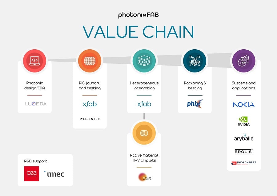
The photonixFAB project calls on Europe-based major public and private enterprises, plus research institutes, to empower photonics innovation by small and midsize enterprises, as well as large entities by providing low barrier access to low-loss SiN- and SOI-based photonics platforms with InP and LNO heterogenous integration capabilities. The visual depicts the initiative participants and their functions within the value chain. Courtesy of X-FAB.
The project is supported by the Key Digital Technologies Joint Undertaking, with funding from EU and European national authorities. The combination of this funding and the investments being directly made by each of the consortium members totals €47.6 million ($51.6 million).
In a press release unveiling the initiative, X-FAB said that the industry-scale silicon photonics manufacturing services that the project seeks to develop will be marked by low entry barriers and fast turnaround times for low-loss SiN- and SOI-based PICs. Another goal will be to enable microtransfer printing and direct bonding technologies for InP-, LNO-, and germanium-based active and passive component heterogenous integration on SiN- and SOI-based PIC platforms. Scalable packaging and testing solutions in alignment with the heterogenous PIC platform developments, as well as process design kit-based design automation enablement for the developed photonic platforms, are other target outcomes.
Six demonstrators are now being built to validate the implemented photonics value chains. These include applications such as datacom and optical switches; coherent optical transceiver; infrared spectrometer for sensing; digital olfaction sensor for consumer health care; and a health monitoring demonstrator. Prospective opportunities for the devices to be fabricated via the photonixFAB project include data- and telecom, biomedical sensors and detectors, quantum computing, and vehicle lidars.
A major part of the work of this 3.5-year project will be conducted at X-FAB’s foundry operation in Corbeil-Essonnes, France, with additional activities also undertaken at the numerous other partners’ sites across Europe.
/Buyers_Guide/X-FAB_Semiconductor_Foundries_GmbH/c20982
/Buyers_Guide/LIGENTEC_SA/c31666
/Buyers_Guide/Smart_Photonics/c30559
/Buyers_Guide/PHIX_Photonics_Assembly/c31818
/Buyers_Guide/Luceda_Photonics/c32297
/Buyers_Guide/Nokia/c33461
/Buyers_Guide/Brolis_Semiconductors/c22171
/Buyers_Guide/PhotonFirst/c17332
/Buyers_Guide/CEA-Leti/c24495
/Buyers_Guide/Imec/c22187