Jeremy Picot-Clemente, European Photonics Industry Consortium (EPIC)
Whether they take the shape of Fresnel lenses and spirals — or something resembling topographical maps, peacock features, or hyperbolas —
diffractive optical elements (DOEs) are designed to introduce a particular phase shift to incoming light to create a desired phase profile of the outgoing beam. They are vital components that find use in a broad range of applications, including beam shapers for laser welding, cutting, and machining systems, as well as beamsplitters for optical telecommunications. DOEs are also a valuable component in optical disc readers and pattern generators for machine vision, and in anti-fraud protection for security documents.
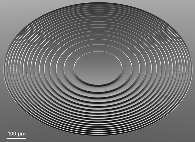
A concave spherical Fresnel lens with a height of 10 µm, a radius of curvature of 840 µm, and an effective diameter of 1 mm. Written with a Heidelberg Instruments DWL 66+ laser lithography tool. Courtesy of Heidelberg Instruments.
The main benefits of DOEs are the high precision, energy efficiency, and versatility they offer by replacing or combining refractive optics with diffractive optics. Additionally, they can be tailored to specific applications to enable precise phase control across the aperture and to create complex intensity profiles.
The performance and attributes of DOEs are closely linked to the method of their fabrication. Understanding the most widely used and promising techniques to manufacture these optical elements can offer insights into the range of possibilities they offer.
DOE fabrication
Diamond machining is among the more familiar fabrication methods. In this process, a computer-controlled diamond tip generates diffractive microstructures by scraping away optical material from a blank.
The advantage of this method is that it can produce a range of high-quality elements, including reflective, transmissive, refractive, and diffractive optical components. One of its drawbacks is that the minimum size and roughness of the component is determined by the dimensions of the tool and the workpiece material. Because the process is also time-consuming, it is used mainly for custom single parts, such as those used for astronomy, as well as mold inserts for mass production by replication. Diamond machining is unsuitable for machining large series, such as consumer products.
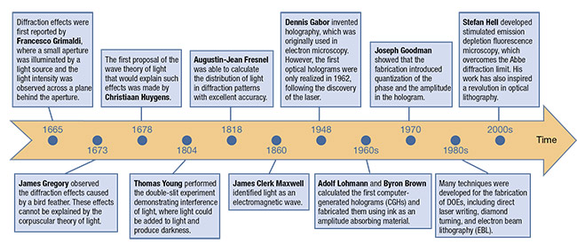
A timeline of diffractive optical elements. Courtesy of EPIC.
Another fabrication method, mask-based lithography, derives from the electronics industry. In a typical approach, a photoresist layer is deposited on a substrate by spin coating and then selectively exposed to ultraviolet light through a binary mask of alternating transparent and opaque areas. The transparent sections cause a selective chemical change to the photoresist, which allows removal of the resist to form a specific pattern that can be etched into the substrate until a required depth is reached. The photo-resist pattern is then removed, resulting in a binary or two-level diffractive optical element.
SUSS MicroOptics SA, based in
Switzerland, manufactures high-quality
refractive, diffractive, and imprint
(polymer-on-glass) micro-optics. It offers
custom development, prototyping, and volume production of elements for optical communications, lighting, and laser processing based on semiconductor processing and imprint techniques. Axetris, another Swiss company, makes customized micro-optics and diffractive optical elements used in transceivers and switches in communications, 3D sensing, and lidar, and for beam shaping in industrial or medical applications. Axetris also offers wafer-level microfabrication and MEMS processing features for assembly and integration, or as post-processing on customer CMOS wafers ranging from prototypes to high volumes.
Grayscale lithography eliminates
the mask and instead scans a laser
beam directly across the surface of a
photoresist-coated substrate. The exposure depth at each position is precisely controlled by modulating the laser intensity. The technique can easily fabricate microlens arrays, multilevel DOEs,
Fresnel lenses, diffusers, and other
complex surfaces.
Grayscale lithography sometimes faces challenges from stitching effects or nonlinearities. But advanced techniques, such as multipass exposures and optimized gray-value distributions, can often provide solutions. Electron beam lithography (EBL) applies a similar principle as serial direct-write lithography, except EBL uses an electron beam for exposure.
To avoid electric charging, a metallic layer — usually chromium — is deposited on the substrate via sputtering before the photoresist spin coating step. The photoresist layer is then exposed directly (without a mask) and sequentially to
produce the DOE pattern by moving the
coated substrate accordingly on a two-dimensional translational stage. EBL can fabricate structures between 20 and 200 nm in polymethyl methacrylate (PMMA) photoresist, depending on the resist’s thickness. The main drawbacks of the technique are its high cost and the slow exposure process, which results in writing times that can take several hours to expose areas of only a few square millimeters.
Additive manufacturing
Two-photon polymerization (2PP) is an additive manufacturing technique that enables freeform 3D writing of polymer microstructures in transparent photo-
resists. 2PP is a direct-write technique
(i.e., without the use of photomasks) that relies on a two-photon absorption process of the write beam to excite a molecule from one energy state to a higher state. The phenomenon results in a chemical
change (usually polymerization) at the focal volume of the write beam. By scanning and properly modulating the write beam, an arbitrary 3D pattern can be polymerized in the material, which can then be developed in a chemical solution to create a fully 3D structure.
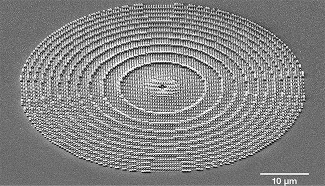
An example of a computer-generated hologram that creates a top hat diffuser. Courtesy of SUSS MicroOptics.
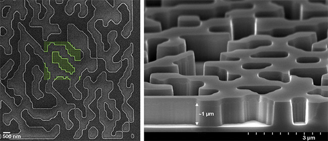
A metalens with features down to 100 nm. Developed as part of the EU-funded PHENOmenon project, grant agreement
No. 780278. Courtesy of Multiphoton Optics.
Heidelberg Instruments, which
acquired SwissLitho in 2018 and
Multiphoton Optics in 2021, recently introduced 2PP technology based on Multiphoton Optics’ MPO 100 direct laser writing system. This system generates meta-atoms to make metamaterials with
a diameter down to 100 nm in a single
process step. As a result of its nonlinear absorption, 2PP provides feature sizes below the diffraction limit and can vary both the diameter and height of meta-atoms, thus adding an additional degree of freedom in design for polymer-based metalenses. Furthermore, the use of
optical polymers means that the applications can be used as a functional
structure or as a master for replication technologies.
Thermal scanning probe lithography
Thermal scanning probe lithography is another direct-write nanolithography technique, in which patterns are created by scanning a nanometer-sharp heated tip over the sample to sublimate a thermal resist locally. This technique can provide grayscale patterns with a precision of 2 nm in depth. The depth of the written pattern is determined by the tip temperature and the applied force. The latter is controlled by closed-loop lithography. Both discrete and continuous grayscale patterns are possible — compatible with subsequent etching, template stripping, soft molding, and nanoimprint lithography.
To an infinity of applications and beyond!
DOE applications include almost all of the applications of conventional optics, as well as a huge range of a nonstandard optical applications. Lighting, telecom, medical, display, sensing, and AR/VR are markets in which DOEs find application and even improve them as compared with conventional optics solutions. DOEs are also needed in applications such as lidar, 3D sensing, optical computing, laser machining, imaging systems, displays, barcode scanning, illumination systems, position encoders, data storage systems, photolithography enhancement, optical communications, and biological sensors. This is by no means a complete list of applications for which DOEs can be used and provide solutions.
With recent developments in fabrication technology enabling nanoscale features, precise and high-quality DOEs promise to improve the performance of optical applications while reducing the complexity and number of conventional optical elements.
An image captured by a near-IR camera with an f/# of 1.6, based on a single meta-optical element. Courtesy of NIL Technology.
NIL Technology, a Danish optical solutions company that replicates and nanoimprints complex nanostructures, has been designing, prototyping, testing, and manufacturing flat optics for more than two decades. The company can now combine metaoptics and diffractive optics to build thinner, flatter, and lighter solutions compared to the possibilities of refractive lenses.
Carried by growing markets — such as 3D sensing for consumer electronics,
AR/VR technologies, and lighting
systems for automotive — DOEs are
helping designers to miniaturize light sources and reduce thickness, weight,
and material consumption while adding
new optical functions, invisibility of optical structure, and increased efficiency. There is no doubt that these DOE technologies will bring new technological opportunities.
Metalenses — from the Greek word “meta-,” meaning “to go beyond” — are already a revolution in diffractive optics. These optical metasurfaces are thin diffractive optical elements, fabricated using standard micro- and nanofabrication techniques. They provide new ways of controlling the flow of light based on various properties such as polarization, wavelength, and propagation direction.
In addition, their compatibility with
standard microfabrication techniques
and their compact form factor enable the development of several novel platforms for designing and implementing complicated optical elements and systems. Metaoptics has attracted widespread attention and was hailed as one of the
top 10 emerging technologies of 2019 by the World Economic Forum and Scientific American. There is no doubt that the
optical revolution is on track.
PHABULOuS: The European Pilot Line for Freeform Micro-Optics
In 2018, an EU-funded consortium of
19 companies and research organizations was formed to create the infrastructure for a self-sustainable pilot line for the manufacture of freeform microlens arrays.
The initiative, known as PHABULOuS, is led by the Swiss research and technology organization CSEM and focuses on delivering highly advanced and robust manufacturing technology for optical freeform microstructures.
The consortium has two basic aims. The first is to strengthen Europe’s position as a technology and machine provider for the production of freeform micro-optics, based on a value-selling model that retains the high-cost and high-value technology portfolio in Europe. The second is to develop easily accessible, world-class manufacturing facilities so that European companies can use micro-optical components in their products and compete advantageously on a global scale. For more information, visit www.phabulous.eu.