ANDRÉS F. LASAGNI, TECHNISCHE UNIVERSITÄT DRESDEN AND FRAUNHOFER IWS
A wide range of products — from LEDs to solar cells to medical implants — can be improved through the use of micro- and nanostructures that significantly influence the physical properties of their surfaces. Such topographies can be utilized to functionalize surfaces and adjust their friction, wear, light management, biocompatibility or other properties to the specific requirements for a certain application. These micro- and nanostructures will have an impact on industrial applications only if they can be produced at high fabrication speed with low fabrication costs, and a new processing method called direct laser interference patterning (DLIP) meets both needs.
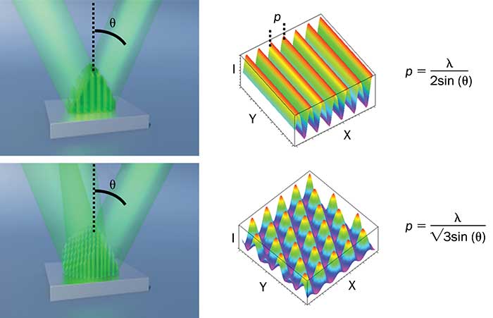
Figure 1. Calculated intensity distribution for two-beam and three-beam interference patterning. The geometrical configurations of the beams necessary to achieve the displayed geometries are also shown. Courtesy of Fraunhofer IWS and Technische Universität Dresden.
Periodic pattern formation
Traditionally, very few technologies have been capable of producing micro- and nanostructured surfaces on large areas. One is laser interference lithography (LIL). In LIL, the standing wave pattern that exists at the intersection of two or more laser beams is used to expose a photosensitive layer, also known as a resist. In the case of a negative resist, the positions that correspond to the interference maxima are photopolymerized. After subsequent resist development, a periodic variation in the surface topography is obtained. However, the multistep character of LIL negatively influences the processing cost and only permits the processing of planar surfaces.
To overcome this problem, pulsed-laser systems with sufficient power and/or pulse energy can be used to directly ablate the surface of the material; hence the name direct laser interference patterning. Similarly to LIL, this technique enables the formation of periodic patterns with different features and defined long-range order. Depending on the number of laser beams that are used, and their geometrical arrangement, different surface geometries can be produced. A two-beam setup, for example, produces a line-like interference pattern, while three beams enable a dot-like geometry (Figure 1).
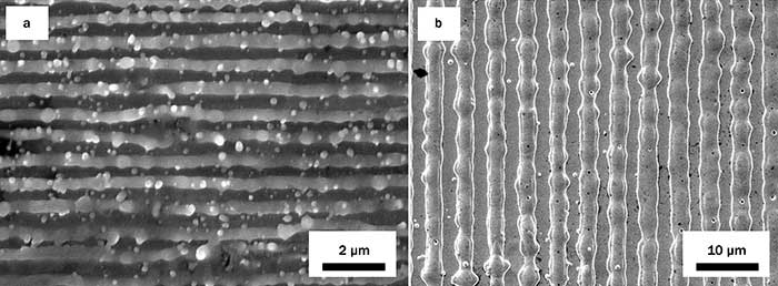
Figure 2. Structured stainless steel substrates using two-beam interference patterning using (a) picosecond and (b) nanosecond laser pulses. The spatial periods are 0.7 µm and 5.0 µm for (a) and (b), respectively. Courtesy of Fraunhofer IWS.
The most important requirement for the fabrication of periodic structures with the DLIP method is that the material being processed must be able to absorb the energy of the laser at the selected wavelength. If high-power laser systems are used, it is possible to achieve fabrication speeds of up to about 1 mm2/min.
The structuring process is based on photo-thermal, photophysical or photochemical mechanisms, depending on the material type. In general, polymers and ceramics are processed with UV laser radiation, whereas green or IR lasers are applied to treat metals and coatings.
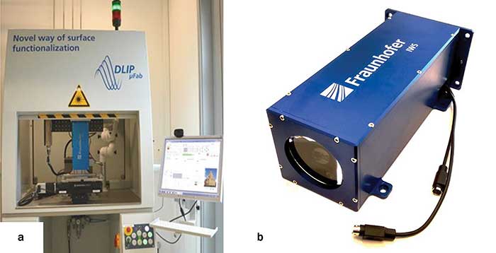
Figure 3. A direct laser interference patterning system (DLIP-µFAB) (a) and a DLIP optical head developed at Fraunhofer IWS and Technische Universität Dresden (b). Courtesy of Fraunhofer IWS and Technische Universität Dresden.
In the case of metals, DLIP is based on a photothermal process that involves local melting and/or selective ablation at the interference maxima positions. For nanosecond laser pulses, the primary material removal mechanism is ablation, but substantial melting occurs. The minimum pitch, or spatial period, is therefore limited by the thermal diffusion length, which is roughly 1 μm for stainless steel and titanium and 2 μm for copper (for 10-ns pulses). When the laser pulse width reduces to the order of picosecond or femtosecond, little thermal damage is observed and pitches below 1 μm are feasible (Figure 2).
At the laboratory scale, interference patterns can be obtained by splitting a coherent laser beam using beam splitters while the beams are later overlapped at the workpiece using several mirrors. Although these optical configurations are acceptable for research purposes, an industrial application of the DLIP technology will only be possible if compact optical-head solutions and systems are available.
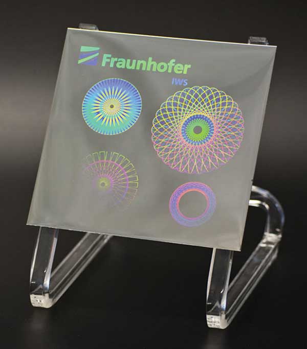
Figure 4. An optical photograph of a decorative element fabricated on nickel substrate using a nanosecond-pulsed IR laser system installed in the DLIP-µFAB machine. Courtesy of Fraunhofer IWS.
Optical concepts and systems
In recent years, different laser interference patterning optical concepts and systems (DLIP-μFAB) have been developed (Figure 3). These systems offer the possibility of processing not only planar surfaces but also complex 3D parts. The optical heads (Figure 3b) can be equipped with different components that control the intercepting angle between two laser beams fully automatically. Consequently, manufacturers can fabricate periodic structures with different spatial periods at different positions. In this way, decorative elements, for instance, can be produced (Figure 4).
In addition to 2D parts, DLIP can be used for the treatment of 3D elements. For this purpose, the DLIP optical heads can be combined with either linear or rotational translation stages or they can be mounted on a robotic arm.
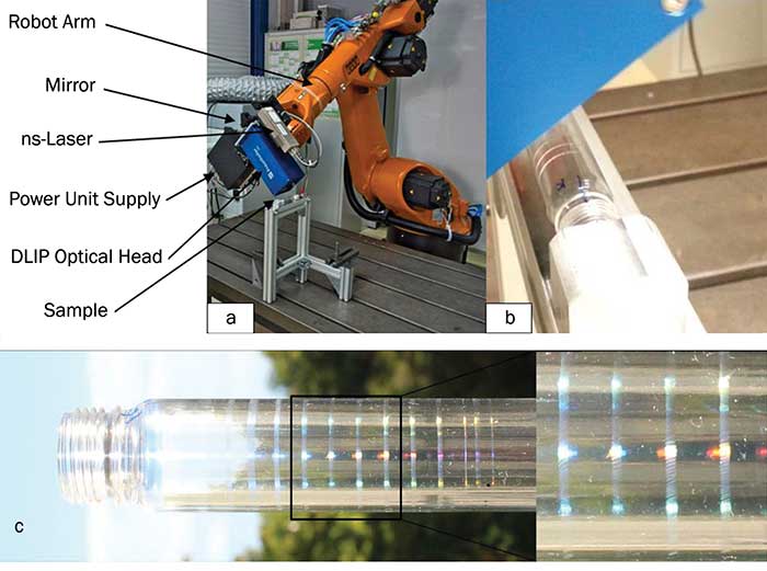
Figure 5. The experimental setup of DLIP using a robot arm. The DLIP optical head is fixed to the robot arm together with the laser system as well as the power unit supply (a). An optical micrograph of the cylindrical polyethylene terephthalate (PET)-treated part and the used DLIP optical head over the cylinder (b). A treated PET cylinder at different positions corresponding to different linear speeds. The inset shows the structures produced at 400 mm/s with a positioning error of ~90 µm (c). Courtesy of Fraunhofer IWS.
3D processing
When combined with linear or rotational translation stages, the DLIP processing head can be translated vertically, and the relative Z-position of the two components can be adjusted. This strategy is appropriate for parts with curvature angles that are less than 20°, corresponding to deviations in the structure period of up to 6.4 percent. If it is necessary to treat 3D parts with larger angles of curvature, an industrial robot can provide the required flexibility (Figure 5a). The main advantages of this system are the large working space — 2033 mm, 2230 mm and 2429 mm — and a maximum linear speed of 2000 mm/s. A 263-nm laser system would be used, for example, because of the high absorption of polyethylene terephthalate (PET) bottles in the UV range (Figures 5b and 5c).
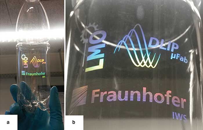
Figure 6. A treated PET bottle using a DLIP-µFAB system (a) and (b). The accuracy of the system is below 1 µm. The system is equipped with 4 axes, including 200 × 200-mm XY translational states and a 360° rotational axis. The DLIP-optical head is mounted over a Z-translational stage with travel length of 100 mm. Courtesy of Technische Universität Dresden.
If rotational symmetrical parts have to be treated, the DLIP-μFAB system can be equipped with a rotational axis. With the processing of a PET bottle, for example, it must be fixed to the rotational axis and be translated with a linear stage and rotated to produce 3D elements, such as holographic pixels, directly on the object’s surface (Figure 6). Due to the high accuracy of the used translational stages and rotation axis, the accuracy between the treated area per laser pulse was approximately 0.5 μm.
Larger parts
When larger parts must be treated, a special DLIP system, developed at Germany's Technische Universität Dresden, can be used (Figure 7). This system treats cylindrical parts up to 600 mm in length and 300 mm in diameter, and is equipped with both nanosecond and picosecond laser systems. Similar to the DLIP-μFAB system, different optical heads can be utilized.
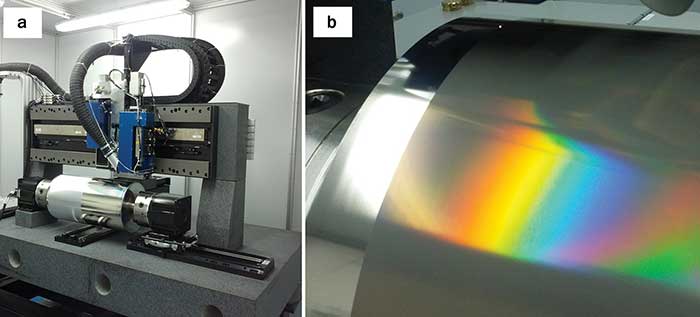
Figure 7. The large area DLIP system for the processing of 2D and 3D parts (a). A 300-mm-diameter nickel sleeve processed with a nanosecond-DLIP optical head (b). Courtesy of Technische Universität Dresden.
These results demonstrate the capabilities of the DLIP method for the production of periodic surface patterns on 2D and 3D parts, with resolutions down to the submicrometer range. Further, these results indicate the high maturity level of the technology and highlight its potential for integration into industrial applications.
Meet the author
Andrés F. Lasagni is the group leader at the Fraunhofer IWS and a professor at the Technische Universität Dresden,
both in Dresden, Germany; e-mail: [email protected].