
DSI Increases Photolithography Patterning Capacity
SANTA ROSA, Calif., March 6, 2013 — Thin-film optical coatings manufacturer Deposition Sciences Inc. (DSI) has introduced a photolithography production line that can pattern 200-mm-diameter wafers.
The patterning capability provides an enhanced view or enhanced detection in multispectral imaging tasks by fusing together information from different wavelength bands.
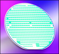
A 200-mm-diameter wafer developed by Deposition Sciences has enhanced photolithography capability. Courtesy of DSI.
“This new manufacturing line brings us better resolution, increased capacity, an ability to yield and coat more parts per wafer, and, ultimately, better pricing for our customers,” said Michael Newell, director of marketing and sales. “And we are keeping pace with the semiconductor industry. Customers are looking to integrate their electronics with the optical filters. DSI can pattern populated wafers containing active devices, and semiconductor fab houses are doing more and more at the 200-mm wafer scale.”
Other applications for the wafers include satellite imaging, machine vision, food and industrial inspection, automotive, biomedical sensing, unmanned aerial vehicle reconnaissance, color filter arrays for CCD and CMOS cameras, and reticles.
For more information, visit: www.depsci.com
/Buyers_Guide/Deposition_Sciences_Inc_DSI/c3580