With advancements in research, and increased traffic in hyperscale data centers, nanophotonic solutions are playing a vital role in fiber optic communication.
HANK HOGAN, CONTRIBUTING EDITOR
Decades of research and development are finally paying off for silicon nanophotonics. The silicon optical transceiver market, for example, is projected to grow nearly twentyfold in volume over the next five years, much of it driven by the needs of large data centers and 5G technology.
In addition, recent lab demonstrations show promise for the miniaturization of optical gyroscopes, lidars, medical sensors, and atomic clocks. These innovations could potentially bring down the cost of these devices while improving both performance and reliability.
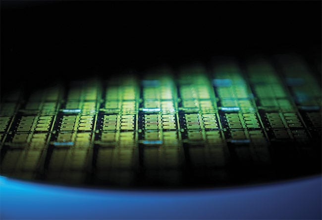
Each of the many hundreds of dies on this 300-mm wafer contains four lasers with different wavelengths, plus modulators, optical multiplexers, and photodiodes. Courtesy of Intel.
Currently, the largest market demand in silicon photonics is for data center interconnects (DCIs), the fiber optic links over which servers exchange information. In a May 2 press release1, Eric Mounier, an analyst at Yole Développement, said the market for silicon photonics optical receivers “will grow from around $455 million in 2018, equating to 1.3 million units, to around $4 billion in 2024, equating to 23.5 million units” — with DCIs by far the largest share of the market.
Fiber optic link applications dominate
Integrated silicon nanophotonic optical receiver chips convert incoming electrical signals into pulses of light and vice versa. Typically produced by an indium phosphide (InP) microlaser, these IR pulses occur at a wavelength that meets application requirements and matches optical fiber transmission qualities.
“Wavelengths around 1310 nm are used in specifications for classic data center reaches of sub-10 km. You’ll typically find 1550 nm used for longer-haul applications,” said Greg Young, vice president and general manager of the optics team at San José-based Cisco Systems Inc. Young was formerly CEO of Luxtera, a silicon nanophotonics company acquired by Cisco in early 2019.
According to Young, lithographic techniques enable micropatterning of gratings and other optical elements in the silicon in a way that is repeatable and precise. This repeatability makes it easy to scale up a device layout and replicate elements across millions of chips.
Some photonic functions, such as light
generation and sensing, require nonsilicon materials — for example, InP for the laser, and germanium (Ge) for the photodetector. These materials are then combined with the silicon chip.
Cisco forecasts a tripling of traffic within data centers between 2016 and 2021, with an increasing percentage taking place in hyperscale facilities such as those built by Google, Amazon, Facebook, Apple, and Microsoft. Hyperscale data centers are designed to be expanded to virtually any size desired. Because of their architecture, these types of centers require high-speed connections to move massive amounts of data between their basic building blocks — the individual servers and their supporting equipment.
Until recently, state-of-the-art transmission rates over links in data centers were 100 Gb/s. Now, the industry is about to deploy 400 Gb/s. And faster speeds are on the horizon. The increase in transmission rates means that silicon nanophotonic solutions will work their way deeper into the communications structure.
Evolving connections
Silicon nanophotonic technology is already found today in system-to-system connections in data centers. In the future, the technology will move into the connections between chips within servers and eventually between sections on the chips themselves. This evolution is a response to the difficulty of moving electrons at higher and higher speeds over shorter and shorter distances.
“Eventually, you move from electrical interconnect and copper to fiber optics,” Young said. At the same time, he added, if the best solution is electrical, that will be what is implemented.
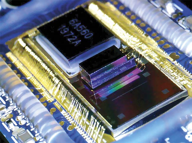
An optical transceiver built using silicon photonics. Today, these link servers together in data centers. In the future, the technology could connect chips or even sections of chips. Courtesy of Cisco.
Thus, for the foreseeable future there will still be a mix of electronics and photonics, and a need to move between the two. According to Young, for a given data rate and distance, the transition from an electron-based approach to an optical approach will happen only when that transmission method has proved to save sufficient power and/or money and boost system bandwidth as well as application performance.
Intel of Santa Clara, Calif., is another leading supplier of silicon nanophotonic
chips for today’s interconnection solutions. The company is producing
100-Gb/s transceivers and will go into production later this year with 400-Gb/s devices, according to Robert Blum, director of strategic marketing and business development for Intel’s silicon photonics product division. He added that Intel is looking beyond, to the next data rate.
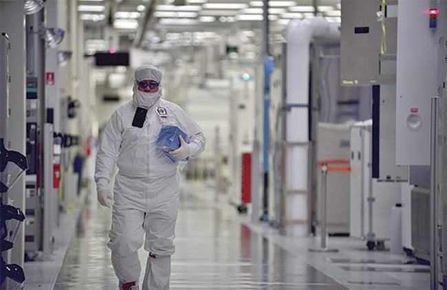
Silicon photonics are manufactured in cleanrooms using lithographic and other techniques derived from semiconductor chip manufacturing. Courtesy of Intel.
Current servers may use up to 32 silicon photonics transceivers at the 100-Gb/s rate for the traffic between servers. The next-generation interconnects will need the same number of 400-Gb/s chips to achieve a quadrupling of capacity. After that, if data capacity increases fourfold as expected, today’s approach of using individual pluggable photonic transceivers with separate microelectronic switches will not work. Instead, small photonic chips, which Blum called “chiplets” or “photonic engines,” will be placed next to the electrical networking chip to integrate photonics and electronics in a single multichip package.
“You cannot do that with traditional optics. You have to use silicon photonics for that,” Blum said of this configuration.
This is because a traditional optical
approach requires too much space and
too many discrete components. Functionally, the traditional and silicon-based techniques are the same, but the silicon-based approach is much less costly to build and offers faster throughput, according to Blum.
Intel uses pick-and-place technology
and wafer bonding to put InP gain
material on a photonic chip while it is still part of a silicon wafer, with the InP grown on a separate wafer. This approach, Blum said, makes it possible to selectively place slightly different InP material to create a photonic chip with wavelength multiplexed output made up of various wavelengths. As it exits the chip, the light is then tapered vertically and horizontally so it couples well with the fiber.

A schematic of a metasurface reshaping a light pulse. Composed of millions of tiny pillars and an integrated polarizer, a metasurface can alter the amplitude, phase, or polarization of each frequency component, allowing pulses to be stretched, compressed, or split. A metasurface can also mimic bulk optics. Courtesy of S. Kelly/NIST.
Intel, he added, is currently focused on the data center market, but is looking at other opportunities. One opportunity is lidar, for which silicon photonics offers the ability to create a more compact optical system with enhanced performance. Optical gyroscopes are another possible application. Potential advancements in the quantum dot light laser — a microscopic light source — could enable photonic chips to be even smaller and consume even less power.
Benefits from research
As commercial use of the technology expands, basic research in silicon nanophotonics continues to move ahead. Recent work performed by researchers at the California Institute of Technology (Caltech) in Pasadena may benefit optical gyroscopes. Scientists there reported in the November 2018 issue of Nature
Photonics2 on a potential performance-boosting breakthrough: a 2- × 1-mm gyroscope that could offer 30× better performance, while being 500× smaller than previous models.
The performance of an optical gyroscope is linked to path length, with a longer path yielding greater precision and less sensitivity to thermal and other noise sources. To overcome these size-related constraints and shrink the gyroscope, the Caltech researchers alternated the light path, flipping it back and forth quickly enough to suppress the effects of the noise.
“We are able to build functional integrated fiber optic gyroscopes,” said Parham Khial, a graduate student and lead author of the paper. “This integration allows for a compact solid-state system with no moving parts, and this may be able to replace or augment current MEMS gyroscopes, where long-term viability is critical.”
The researchers are now fabricating new devices that will offer improved stability and precision. Possible use cases for the devices include drones and self-driving cars. Khial said there have been inquiries about licensing the technology, which is patented.
In another example, researchers from the Gaithersburg, Md.-based National Institute of Standards and Technology (NIST) demonstrated a new way to shape ultrafast optical pulses, as reported in Science3. Their approach could prove useful in silicon nanophotonics, according to Amit Agrawal, a NIST physicist and paper co-author.
They etched microscopic pillars out of silicon to create an array with a characteristic feature size smaller than a few hundred nanometers. To an ultrafast laser pulse centered around 800 nm, the array of silicon pillars forms a metasurface, or an artificial sheet material that can have properties not found in naturally occurring materials. A metasurface can also mimic the properties of optical components such as lenses and wave plates. By arranging the pillars in specific patterns and sizes, the researchers could shape ultrafast pulses in any way they wished: They could compress them, stretch them, split them, change their intensity, or alter their polarization.
Because of the material and method of manufacture, a metasurface approach is compatible with silicon nanophotonics. And the ability to shape and customize beams exiting a chip could prove a valuable tool. Today, this type of beam manipulation is handled only by traditional free-space optics. However, free-space optics are bulky and expensive to assemble, which means the final solution is larger and more costly than would be the case with silicon pillars or another metasurface. What’s more, traditional bulk free-space optics can be knocked out of alignment, something that cannot happen to pillars integrated with silicon nanophotonics.
NIST researchers are working on combining metasurfaces with integrated photonic devices to achieve on-demand shaped optical beams, according to Agrawal. “This is part of the recent push to take free-space, table-top optical experiments such as atomic trapping for atomic clocks to the chip scale,” he said.
Trapping an atom involves multiple laser beams — five or so to hold the atom and one to probe its state and thereby derive time data. Executing this feat on a
chip could cut atomic clock costs significantly while making such devices manufacturable and more robust. Precise time-keeping is important in location technologies, such as GPS. So, more efficient and less expensive atomic clock capabilities could have far-reaching effects.
Currently, metasurfaces and the beam shaping they create are fixed and cannot be changed. But Agrawal said work is underway on “active metasurfaces” that will be able to alter their beam-shaping attributes on command. This capability could be useful in applications such as
on-chip lidar that sweep a beam around.
Finally, in discussing the future of integrated silicon nanophotonics, Intel’s Blum noted that data center applications are of primary commercial interest now. He predicted attention will broaden as new applications, such as gyroscopes and lidar, come online.
“I think it’s a really exciting time for photonics,” Blum said.
References
1. Yole Développement (2019). Si photonics: beyond the tipping point, http://www.yole.fr/PhotonicIC_SiPhotonics_MarketUpdate_Intel.aspx#.XUwfTnspCUm.
2. P.P. Khial et al. (Nov. 2018). Nanophotonic optical gyroscope with reciprocal sensitivity enhancement. Nat Photonics, Vol. 12,
pp. 671-675.
3. S. Divitt et al. (May 2, 2019). Ultrafast
optical pulse shaping using dielectric
metasurfaces. Science, Vol. 364, Issue 6443, pp. 890-894.