Scientific and consumer markets are driving heavy demand for CMOS sensors, and developments such as AI compatibility are at hand.
FAROOQ AHMED, CONTRIBUTING EDITOR
Twenty-five years ago, physicist and engineer Eric Fossum predicted the end of the charge-coupled device (CCD) imaging sensor1. Fossum, a Dartmouth University professor who was then at NASA’s Jet Propulsion Lab just north of Pasadena, Calif., helped develop the first complementary metal oxide semiconductor (CMOS) active pixel imaging sensors. In the intervening decades, Fossum’s prediction came true; CMOS imagers, spurred by high demand in the smartphone industry, have become commonplace in nearly every type of consumer camera and in most scientific imagers as well. More than 4 billion cameras with CMOS imagers are sold each year (Figure 1).
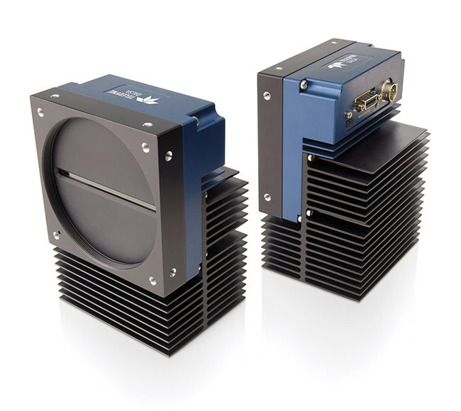
Figure 1. Teledyne DALSA’s Linea HS 16K camera uses a charge domain CMOS TDI image sensor for high speed and high sensitivity in low-light industrial applications. Courtesy of Teledyne DALSA.
CCD vs. CMOS
Suraj Bhaskaran, a senior manager of engineering and R&D at Waltham, Mass.-based Thermo Fisher Scientific, said CCD imagers, invented in 1969 at Bell Labs, were the standard in scientific imaging because of the high quality of their image data. “But what I’ve seen over the past
10 years is that the technology has transitioned,” Bhaskaran said.
Now, high-volume CMOS sensors are driving the scientific as well as consumer markets. “At one point, scientific imagers spurred advances in the consumer sector, but recently that role has been reversed,” he said.
Unlike CCD sensors, active pixel CMOS sensors combine imaging and processing functions on one circuit. “The photoelectric response is more linear,” Bhaskaran said. CMOS sensors have faster response times and lower power requirements than CCDs, and they can be produced in less-specialized silicon-process foundries. “For some applications, sourcing CCDs has started to become a problem, actually,” he added.
Astronomy, for example, had been one of the few disciplines that relied on CCDs more than on CMOS sensors because of CCDs’ low noise and the need for astronomers to integrate thousands of hours of observational data. However, according to Sarah Wu, North America business development manager for the German industrial imaging company FRAMOS, “Even for applications such as astronomy and the life sciences, which were strongholds for CCDs in the past, we’ve seen CMOS sensors starting to penetrate and take over.”
Multistacking
Mark Butler, the product manager for line-scan imaging at Waterloo, Ontario, Canada-based Teledyne DALSA, said one of the main benefits of CMOS sensors is that several components can be manufactured onto one silicon wafer. Early on, analog-to-digital converters were quickly packaged with CMOS sensors, and the integration made digital image production more efficient and cost-effective.
Smartphone component manufacturers have taken this integration a step further by developing multistack chips. Butler explains that a typical 3D-stacked chip may contain a CMOS sensor on one die, an analog-to-digital converter on another, and a final layer with memory. “As smartphone sizes have decreased, stacking offers a compact solution,” he said. Butler expects to see these advancements move into other areas as well, such as machine vision.
FRAMOS, which has been a Sony Corp. distribution partner since 1982, held its annual Tech Days event in Munich in May. At the event, representatives from Sony presented the latest iteration of Sony’s Pregius S CMOS sensor, which will be released in the fall. The new version of the sensor leverages stacking and combines Sony’s proprietary shutter technology with a back-illuminated pixel structure (Figure 2). Reached by email, FRAMOS’ Wu called the advancements “unthinkable” and said, “All applications — from embedded vision applications to 3D reconstruction, inspection, AR/VR, and life sciences — that need higher resolution, faster speed, higher quantum efficiency, and lower noise will benefit from this latest technology.”
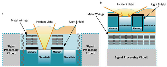
Figure 2. Conventional front-illuminated image sensor with global shutter function (a). Sony’s newly developed Pregius S sensor, a back-illuminated stacked image CMOS sensor with global shutter function, which will be released this fall (b). Courtesy of FRAMOS.
Quantum dots
At Thermo Fisher, Bhaskaran has been exploiting niche applications. These include developing radiation-hardened image sensors to monitor patients during radiotherapy for cancer treatments, and specialized devices with increased dynamic ranges rather than lower noise performances. He is also working on a project to enhance the UV sensitivity of current, off-the-shelf CMOS and CCD sensors using quantum dots. Traditionally, Lumogen-based organic phosphors have been used for this process. The phosphors, however, respond to a wide range of UV wavelengths.
Bhaskaran and researchers at the Rochester Institute of Technology have demonstrated a method of ink-jet printing that deposited tunable quantum dots in a transparent film onto the sensors2. The primary advantage of these quantum dots is they can be tuned or optimized to a specific wavelength. “The applications, for now, would mostly be in scientific fields,” Bhaskaran said.
Bhaskaran serves on the advisory board for the 2019 Image Sensors Americas conference taking place in San Jose, Calif., in October. He said the wide dynamic ranges of current CMOS imagers, as well as their competitive pricing, have contributed to their expansion into new areas (Figure 3). The automotive industry, with its promise of self-driving cars, is one such market. Industrial monitoring using line- or area-scan cameras is another.
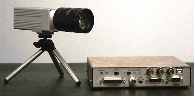
Figure 3. At Thermo Fisher Scientific, Suraj Bhaskaran’s group developed a radiation-hardened solid-state camera system tolerant to 3 megarad. Courtesy of Thermo Fisher Scientific.
Multiline scanners
In May, Teledyne DALSA announced volume production of its new Linea HS line-scan camera for industrial monitoring. The 16K, 300-kHz camera uses a CMOS sensor equipped with time delay and integration (TDI) technology that the company has also deployed in CCD imagers. The camera won gold-level honors last year at the Fourth Annual Vision Systems Design Innovators Awards in Boston.
According to Teledyne DALSA’s Butler, the line-scan camera was designed for use in low-light conditions where high speed and sensitivity are paramount concerns. “This camera can be used to inspect everything from flat-panel displays, PCBs, silicon wafers, and DNA [for] sequencing,” he said. As components have gotten smaller, such as in the smartphone industry, the need for higher-resolution imagers has increased, Butler added.
Multiline CMOS line-scan sensors promise to further aid industrial markets. Four-line sensors could, for example, allow for three-channel RGB color as
well as near-infrared (NIR) scanning. In food inspection, the NIR band could help identify the moisture content of apples during harvest, while in recycling it could help distinguish between different types of plastics, even if they were the same color.
Butler has also seen the use of image sensors in sports and entertainment take off as 4K cameras and displays have become increasingly common. In sports, many professional and some college teams have started collecting and analyzing video of nearly all their games and practices. Data-driven sports, first called sabermetrics in baseball, require high-resolution cameras that can capture video from multiple angles, he said, allowing organizations to pinpoint areas in which teams and individuals need improvement. While the entertainment industry has always required multiple cameras for recording special effects scenes, the proliferation of streaming services such as Netflix
and Hulu has created new avenues for content creators who require sufficient high-resolution equipment with which to shoot.
Personalized medicine is another area that has seen explosive growth for CMOS sensor use. The popularity of direct-to-consumer personal genome testing has led to an increased need for DNA sequencers that rely on high-speed image sensors. “The genomics industry has a 20% per year annual growth rate at the moment,” Butler said.
Printed CMOS
Thermo Fisher’s Bhaskaran sees several trends that will further transform the image sensor industry. The development of new and more cost-effective manufacturing methods is one. Printed and organic electronics, for example, could decrease costs and allow for nontraditional sensor geometries.
Manufacturers such as ISORG have developed organic photodetectors that can be deposited on flexible plastic or glass substrates. ISORG is focusing on large-area applications rather than the small photodetectors that are being developed in personalized medicine applications. Its sensors can also be produced at room temperatures and ambient pressures, unlike the manufacturing processes that often occur in specialized foundries.
In September 2018, the Grenoble, France-based company raised $27.1 million to increase production of commercial devices. It also took part in the European Union’s LORIX Horizon 2020 project, which sought to create large-area x-ray detectors for security, health, and industrial applications by combining organic electronic technologies with existing active-matrix thin-film transistor arrays.
Sensor-side computing
Another development that will affect image sensor technology is the need for data processing and machine learning to occur at the chip level. Just as CMOS sensors combined imaging and processing functions on one circuit, next-generation imagers will need to integrate to be able to make decisions quickly. “IoT, the Internet of Things, already demands communications connectivity in sensors,” Bhaskaran said. “But, increasingly, they’ll need to be able to make choices, too.”
Rather than sending data to a central processor as CMOS sensors do now, newer sensors will be compatible with AI. This added ability will allow for the robust performance and uptake of imagers in industrial or automotive applications. “Any car today has a half dozen or more cameras. What’s going to change dramatically in the next few years is that those imagers will be able to make a decision right at the detection point — potentially saving lives,” Bhaskaran said.
FRAMOS’ Wu added that its AI division is “focused on building custom
solutions to enable productization for
customers.” At the Tech Days event, FRAMOS AI experts made joint presentations with representatives from Santa Clara, Calif.-based Intel about intelligent image processing and depth sensing using Intel’s Movidius line, which it acquired in 2016.
Sensor-side computing, as it has been termed, may have unforeseen consequences, however. In May, Shanghai-based SmartSens Technology, a global supplier of CMOS imagers, announced its SmartSensor AI image chip that integrates
artificial intelligence into a CMOS sensor
to perform local machine learning. Privacy advocates fear that such technologies, when combined with facial recognition algorithms and third-party data mining, could contribute to surveillance states rife with potential for misuse.
Acknowledgments
The author would like to thank Suraj Bhaskaran, Thermo Fisher Scientific; Sarah Wu, FRAMOS; and Mark Butler, Teledyne DALSA.
References
1. E.R. Fossum (July 12, 1993). Active
pixel sensors: are CCDs dinosaurs? Proc
SPIE, Vol. 1900, pp. 2-14, https://doi.org/10.1117/12.148585.
2. A. Knowles et al. (May 13, 2019). Incorporating quantum dots in a magnesium
fluoride matrix to enable deep-UV sensitivity for standard silicon based imaging
detectors. Proc SPIE, Vol. 10982, https://doi.org/10.1117/12.2517865.