The CCD camera is becoming the imaging method of choice in biological laboratories for its resolution, versatility and ease of use. Choosing the best CCD for a given application, however, requires knowing how basic chip parameters affect performance.
Butch Moomaw, Hamamatsu Corporation, Systems Div.
Since their invention in the late 1960s, charge-coupled devices, also called CCDs, have found widespread use in imaging applications. Electronic cameras based on CCD technology are used in applications from home video to medical imaging to astronomy. CCD cameras offer several advantages over film cameras: They can be connected directly to a computer, can be highly sensitive to low-light levels and their images are instantly available without film or dark-room processing.
As their costs come down, CCD sensors are becoming essential tools for microscopists and biologists, though many users know very little about their actual characteristics and operating methods. Anyone planning to buy one, however, needs to understand the basics of the technology to know which type best fits his or her needs.
A CCD chip is an array of photoelectric detectors built on a silicon base using layers of electrical components, called the architecture, printed on the surface. This structure divides the base into a grid of separate compartments, called pixels, that hold electrical charges. A pixel is described by its size and the number of electrons it can hold. The size of a pixel varies from about 6 to 25 µm, and the capacity, called full-well capacity, varies from about 10,000 to 500,000 electrons.
The chip provides a two-dimensional array of photodetectors that convert incoming photons into electrical signals. These signals are then sent to a display where they are reconverted into an image or to a storage device for future reconversion. This conversion and recreation process overcomes some of the limitations of the human eye and transfers data without using photographic processes.
This device can record information outside the range of human vision — from x-ray and UV wavelengths through the visible to the near-IR. A CCD also can have extremely short exposure times that can stop moving objects, and it can integrate over long periods to accumulate images that the eye cannot detect. It has a much lower resolution than the eye at equal magnifications, however, because each pixel is larger than the eye’s rods and cones, which are about 1.5 µm in the area where the eye has its highest acuity.
Each chip has characteristics that are determined by the design and placement of the electrical components of the chip’s architecture. Since these components are on the surface, they absorb light and reduce the efficiency with which the device converts photons to electrons. Different chips exhibit different spectral characteristics — that is, they respond to different wavelengths of light with different efficiencies. They also exhibit different noise characteristics and speeds in transferring the data in the pixels to the display device or computer.
Analog signals
The method of getting the data from the pixels into the display device may be either analog as in a standard video camera, or digital as in a direct computer interface. The chip itself, however, produces an analog signal. This signal, which is composed of the electron charge associated with each pixel, passes through an amplifier and then is transmitted either to another analog device such as a video monitor, or to an analog-to-digital converter so it can be sent to a computer.
An analog signal connects easily to many devices already in most laboratories, such as video monitors and VCRs. However, analog signals come with real disadvantages: Video cables and accessories have higher signal losses, and video standards limit resolution, especially in the vertical direction.
A digital signal has zero loss during transmission, and only the size of the computer’s memory limits the resolution of the image it can handle. The disadvantage of a digital signal is precisely the same as its advantage: Unlike video, there is no standard interface. Therefore, each detector requires a dedicated software interface to transmit the image to the computer. Once in the computer, it must be reconverted to analog for display on the computer monitor. All display devices are analog and are limited to 256 levels of gray, whether the camera is digital or not.
By itself, raw sensitivity, the ability of a detector to record the presence of a photon, is not a good measure of the ability of a camera to make a high-quality image. More important is the combination of properties used to describe a CCD. These properties produce the signal-to-noise ratio figure that describes the ability of a CCD to differentiate between the electrons produced by incoming photons and extraneous electrons caused by noise factors.
One method for improving the overall signal-to-noise ratio sensitivity of almost any CCD chip is to cool it. Cooling reduces the dark noise (electrons created by heat rather than incoming photons). Cooling can be accomplished using circulating water, liquid gases or a thermoelectric cooler, which is a type of electric heat sink that can reduce the temperature of the chip. Every 8 °C of cooling reduces the dark noise by half. Advantages of the thermoelectric cooler are that it can be integrated into the CCD camera package and it doesn’t require continual additions of evaporating cooling materials.
When light hits the chip
Light falling on a CCD chip creates an electric charge in each pixel directly related to the amount of light that fell on that pixel. In a process known as readout, information on the chip is converted to an analog signal. Readout sequentially transfers the charges in each row of pixels, row by row in vertical order, to the row of pixels at the top or bottom of the chip. This row, called the readout row, is blocked from the light by an opaque mask. The transfer is about 99.999 percent efficient and requires only a few microseconds per row.
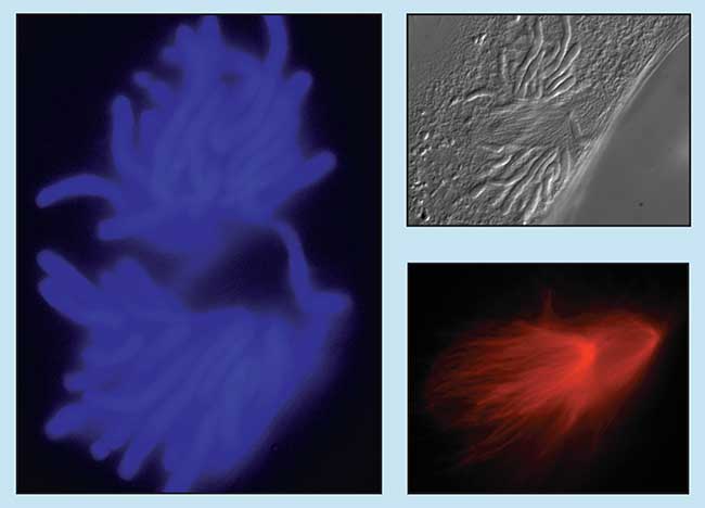
Microscopists regularly employ CCD cameras to collect images using a variety of contrast enhancement methods. Differential interference contrast (upper right) reveals fine structural details in a newt epithelial lung cell, while rhodamine (lower right) turns structural actin filaments red, and the blue fluorophore, DAPI, (left) labels the cell’s chromosomes. Courtesy of Ted Salmon, University of North Carolina, Chapel Hill.
Once in the readout row, the charges proceed horizontally through an amplifier to create a signal that represents one horizontal line in the image. The sequence is repeated until all the rows are transferred and the entire image has been read out. To speed up the readout some chips have more than one readout row, called multiple taps. Extra rows require extra amplifiers that may increase costs and can cause different gray levels in portions of the image.
Light must not reach the detector during readout or it will produce effects similar to advancing the film in a camera while the shutter is open — blurring, image shading or mixing images. The solutions to this problem can affect the suitability of a particular CCD for an application. Each method has advantages and disadvantages.
Readout methods
The most common method of protecting the image is a mechanical shutter, similar to shutters on a regular film camera. The shutter opens for a specified time and then closes. Readout occurs while the shutter is closed. Chips designed for this type of readout are usually called full-frame transfer chips. Almost all CCD cameras use this method, and it is possible to image most stationary objects in both high and low light levels with this type of camera.
This chip is also the primary type available for high-resolution applications requiring pixel arrays larger than 1000 × 1000. Its efficiency makes it suitable for low-light fluorescence applications but it requires that the microscope and mounting method be very stable. This type of chip is generally very good at detecting red and infrared light because it is spectrally more sensitive to longer wavelengths. However, the reduced sensitivity to shorter wavelengths necessitates fairly long exposure times that limit its use for fluorescence applications such as calcium ratioing and green fluorescent protein marking. Because most of these devices have large full-well capacity, they are good for detecting small changes in bright signals or for measuring subtle changes in intensity.
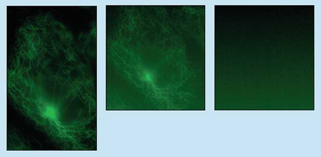
Cooling a CCD chip (right) reduces the thermal noise contribution (left) to an image that otherwise would be harder to read (center). Green fluorescence labels the filamentous actin in a female kangaroo rat kidney cell stained with Alexa 488 Phalloidin. Courtesy of Ted Salmon, University of North Carolina, Chapel Hill.
Another method, called frame transfer, uses a special chip with two identical CCDs paired up; one is exposed to light and the other is entirely masked. Since the row-by-row transfer is fast compared with the actual readout, the second chip provides a place to store the image by shifting it quickly off the exposed chip and then reading out the second chip at a slower pace.
Frame-transfer CCDs have almost the same applications as full-frame-transfer units but can operate at faster speeds. For users who need to acquire pairs of images in rapid sequence or multiple images of areas that are less than the full area of the chip, it is possible to rapidly transfer small subregions of the exposed chip to the masked area (see binning and subarray). This could make it possible to capture four regions of 256 × 256 pixels or 16 regions of 128 × 128 pixels quickly on a chip that has 1024 × 1024 pixels on the primary chip.
A third method, called interline transfer, alternates columns of exposed pixels with columns of masked pixels to provide temporary storage only one pixel away from the imaging pixels. Transferring an image to the masked portion requires only a few microseconds, and all imaging pixels experience the same exposure time.
Two types of interline transfer chips are available. The first is an interlaced interline transfer chip that is used mostly in standard video cameras and camcorders. The second type, the progressive scan interline transfer chip, is used primarily in high-resolution, high-dynamic-range cameras of the type suitable for high-resolution biological imaging.
Recent developments in interline chips have almost eliminated the problems of older interline devices. The first improvement is the addition of on-chip lenses that refract the photons that would normally fall on the masked areas into the imaging pixels. This increases the active area to more than 70 percent. A second development, the hole accumulation device, has reduced the noise levels in the chip so that with minimal cooling, it is effectively noise-free. With such low noise, the device can image a wide range of intensities with a high signal-to-noise ratio from a smaller full-well capacity than many of the older full-frame-transfer and frame-transfer chips.
These chips are more sensitive to shorter wavelengths than full-frame-transfer chips are, at the expense of performance in the red regions. The chips’ exposure times are fast enough to image rapidly moving objects. For brightfield and differential interference contrast applications, they offer fast operation and good stop action for particle tracking and microtubule assembly imaging.
These chips require less cooling and make it simpler to produce good images in low-light applications. They lack the large full-well capacity required to detect small changes in a bright signal, for instance, when imaging voltage-sensitive dyes. On the other hand, their very low noise characteristics are useful for detecting small signals against a dark background.
Binning and subarray
Most CCDs share two capabilities that make them very versatile for scientific imaging: binning and subarray. These properties can increase readout speed, decrease exposure times or reduce the total amount of information that has to be transferred to the computer.
The term binning refers to pooling together the electrons in a group of neighboring pixels. The result is sometimes called a superpixel, and it can be used to shorten exposure times and increase the signal-to-noise ratio at the sacrifice of spatial resolution. Because it produces fewer data, it increases transfer speeds. The camera’s software controls the size of the superpixel, which can include any number of pixels in either the horizontal or vertical direction. In imaging, it is convenient to use equal numbers in both directions to avoid distortions. In spectroscopy, making unequal vertical and horizontal numbers allows the user to take advantage of the orientation of a monochromator’s output.
The term subarray refers to using only a portion of the total CCD area to image a small region of the full view. This is accomplished from within the software controls by drawing a box around the region of interest within the image to specify certain pixels on the CCD. It does not change the resolution of the smaller area, but it greatly reduces the total amount of data that have to be read out and transferred, and thereby increases the speed.
Silicon cannot tell the difference between electrons produced by photons of different wavelengths, so additional steps are needed to create color images. Several schemes have been devised to achieve this.
There are two methods to resolve different colors on a single chip. One is to apply a special mosaic filter composed of an alternating pattern of either red/green/blue or cyan/magenta/yellow spots to the surface of the chip. Applying a mathematical equation to the gray values of each pixel recreates the original real-color image. This information is encoded into the video signal, and the display device or frame grabber reconstructs the image.
The second method uses a rotating filter wheel to expose the entire chip sequentially to red, then green, then blue, with readout occurring between each exposure. This generates three separate images that must be reconstructed by a computer or other hardware memory device.
Another solution is the three-chip color camera that simultaneously captures a red, a blue and a green image on each of three chips through an arrangement of prisms that act as chromatic beamsplitters. The result is three separate but simultaneously acquired images that can be displayed on a regular video monitor or sent to a computer as a standard RGB signal.
The CCD camera has proved useful to biologists in the laboratory because of its versatility and ruggedness. In addition, its sensitivity and ease of use are continuing to win the accolades of scientists who would rather spend laboratory time concentrating on science than on processing photographic film. As chip manufacturers and camera companies continue to develop better devices with higher resolutions, the CCD camera will continue to find a home among laboratory equipment.
Parameters to Consider When Choosing a CCD Camera
• Array size – the number in each horizontal row by the number in each vertical column (e.g., 1024 x 1024). A greater number of pixels is useful for either better spatial resolution (to image fine details) or a larger field of view.
• Pixel size – the actual size of each light-detecting element of an array, measured in horizontal microns by vertical microns. Larger pixels work with shorter exposure times at the expense of resolution, and smaller pixels provide better spatial resolution but require longer exposures.
• Interscene dynamic range – the range of total exposure values from the brightest light level possible to the dimmest light level at which the detector can produce a signal, expressed in lux or photons per square centimeter per second.
• Dark noise – the number of electrons the chip produces at a given temperature when no light falls on it, expressed in electrons at a stated temperature in degrees celsius per second.
• Readout noise – the number of electrons produced during readout that are not related to the signal, expressed in electrons.
• Readout speed – the speed at which the pixels are read out through the amplifier, expressed as pixels per second.
• Quantum efficiency – the fraction of those photons that strike the detector that are converted to electrons, expressed as a percentage.
• Full-well capacity – the maximum number of electrons a pixel can hold. Larger numbers tend to increase the dynamic range within an image and the ability to discern small signal changes in strong signals.
• Intrascene dynamic range – the range of possible intensities within a single image, calculated as the full-well capacity in electrons divided by the noise in electrons.
• Analog or digital – the form of the camera’s data output. The output from earlier cameras was always analog, but most cameras now come with an analog-to-digital converter built in. The gray-scale resolution of the digital output depends on the number of bits in the A/D converter – 8 bits equals 28, or 256 gray levels; 10 bits equals 210, or 1024 gray levels; up to 16 bits, which is 216, or 65,535 gray levels.
• Spectral characteristics – how the color of a photon affects the detector’s response, expressed as a graph of either quantum efficiency of relative sensitivity vs. wavelength, with no noise factors included.