Charge-injection device (CID) technology provides a means to convert optical signals from 185 nm to 1100 nm to electronic charges that can be read out as a video signal or processed via computer. The CID imagers also are capable of directly (or indirectly) converting particle photons including electrons, ions, x-rays and other forms of ionizing radiation to measurable levels of electronic charge.
Tony Chapman, Thermo Fisher Scientific Inc., CIDTEC Cameras & Imagers
Charged-injection device imagers are metal-oxide semiconductor (MOS) detectors that can be fabricated using PMOS, NMOS and CMOS integrated circuit technology, and may be configured as a single-element, linear device or two-dimensional pixel arrays. Individual pixels are formed by coupled MOS capacitors sharing the same row and column electrode (Figure 1). Incident light on the surface of a pixel is converted to a proportional amount of signal charge that is collected and stored beneath the pixel surface. Pixel readout occurs by sensing the charge transfer between the capacitors within the pixel site. Injection of charge into the underlying device substrate clears the pixel, or a lateral injection drain is utilized in preamplifier-per-pixel devices which clears the charge within the pixel.
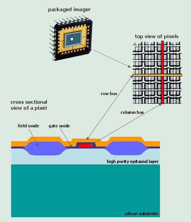
Figure 1. Fabrication of a charge-injection device (CID).
The charge-injection device is an X-Y addressable structure. Single pixel readout, subarray readout or collective read (binning) of pixels is initiated by selecting/driving one or more columns and sensing the combined signal on one or more intersecting rows. Low-noise preamplifiers are incorporated on-chip at the ends of rows (or columns), or, they are embedded within the pixel structure (Figure 2).
Charge-injection devices can be fabricated on various high-purity substrates depending on the application requirements. For instance, an n-type epitaxial substrate is used when high radiation tolerance is desired. Injection of charge into the underlying device substrate or a lateral inject drain for facilitating backside thinning has been implemented for clearing the charge within a pixel.
Charge readout is nondestructive because the charge physically remains within the pixel during readout. Combined with the X-Y addressable structure, this permits true random pixel addressability, allowing a vision system or the camera to read out only the areas of interest to obtain data at faster local frame rates. Moreover, the pixel information can be read out during exposure in a nondestructive read out fashion to optimize signal quality and extend linear dynamic range. These features provide the option to simultaneously read out a group of pixels collectively and enhance signal quality. Furthermore, an algebraic addition of charge packets can be completed on-chip to facilitate a color encoding or readout of a mathematical transform.
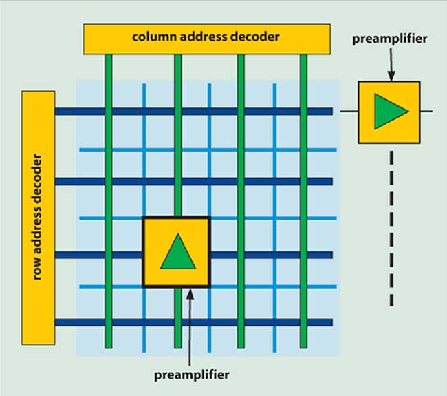
Figure 2. Preamplifiers can be embedded within the pixel structure.
A single charge transfer within the pixel is required to initiate readout, making the device insensitive to charge transfer inefficiencies when compared to other charge transfer devices such as CCDs. Rather than fail catastrophically when exposed to ionizing radiation, key threshold and isolation parameters increase and are dynamically compensated. These features, along with n-type epitaxial material, provide an extremely high level of radiation tolerance allowing CID-based camera products to operate in radiation environments orders of magnitude beyond what competitive technologies can offer.
The charge-injection device pixels contain silicon photogates that are transmissive to light. Since a charge transfer register is not required, the structure allows for large pixel charge storage capacity and a natural broad spectral response (UV through near-IR wavelengths). In addition, the contiguous pixel structure provides a high-quality video signal that facilitates subpixel interpolation calculations and the attendant precise measurement of image features to a fraction of a pixel.
Market needs
Applications in semiconductor, scientific, industrial, aerospace and medical markets require accurate linear photon-to-charge conversion. Features and positions of objects within the total image field must maintain their perspective in the output video signal. Also, it is important to maintain the relative brightness or intensity of objects within the captured image by providing a proportional video output signal. Charge-injection devices meet these basic requirements. They provide good quantum efficiency (especially in UV), excellent linearity and modulation transfer function, and add minimal noise to the signal during the conversion process.
Scientific applications may place additional constraints on imaging detectors used for spectroscopy, x-ray imaging and photon counting. For example, spectroscopy measurements often require very large pixel charge storage capacity so the output signal is quantum or shot-noise limited. Additionally, pixels (or subarrays) may need to be randomly addressable, since each pixel or subarray performs the function of an individual photomultiplier tube.
In spectroscopic applications, spectral line intensity may vary dramatically among the various pixel locations. Antiblooming performance is critical where pixel(s) associated with an intense spectral line must not interfere with that of a less intense spectral line. Imagers used in x-ray applications may require special conversion coatings or may need to be fabricated on special high-resistivity substrates dependant on x-ray energy levels. In both applications imagers may be subjected to intense radiation. Charge-injection devices offer strong antiblooming performance from intense signals and inherently resist the ionizing/drift and damaging effects caused by ultraviolet and x-ray radiation that might accompany these applications.
In many industrial applications, imaging detectors must operate in hostile environments. Charge-injection devices have proven to be an economical, reliable, solid-state imaging replacement for tube technology in robotics, monitoring and diagnostic systems for nuclear power generation, waste disposal and medical applications since they’re tolerant to the effects of ionizing radiation. They continue to function beyond 3 Mrad total dose exposure in flux rates well beyond 1 Mrad/h.
Selective imaging
Industrial applications often require inspection of parts at high frame rates. Charge-injection devices can read out only the portions of the image of interest and offer the possibility of minimizing computer processing of nonessential information and maximizing parts inspection rates.
Aerospace applications may require resistance to image distortion caused by bright spots within the image (blooming). For example, astronomy and tracking applications use the subpixel charge collection characteristics of a charge-injection device to measure area centroids of stars or missile plumes to subpixel accuracy. Blooming from an intensely illuminated pixel would drastically affect the accuracy of that calculation.
In tracking applications, charge-injection devices provide meaningful information at extremely high rates by reading out only regions of interest, an important consideration in terminal homing applications where closing velocities may be very high. And, in some astronomy applications, charge-injection device subarrays can be read out at high rates in order to create a speckle image from individual light photons.
Dental imaging is an area that has embraced charge-injection device technology as an alternative to film. Here, as in spectroscopy, charge-injection devices offer superior resolution and sensitivity because large pixels, with attendant large charge storage capacity, are needed to render quantum-limited operation in radiation-intensive environments.