At the chemical level, diamonds are no more than carbon atoms aligned in a 3D crystal lattice. Even a diamond that looks flawless contains defects that can absorb or emit light. Small defects in diamonds called nitrogen-vacancy (NV) centers hold electron spins that can be manipulated at room temperature. Each NV center emits light that can provide information about the spin’s quantum state.
Collecting light from deeply embedded NV centers usually requires a bulky optical microscope in a highly controlled laboratory environment. Now, a research group at the University of Pennsylvania has designed a specialized metalens that circumvents the need for a large, expensive microscope.
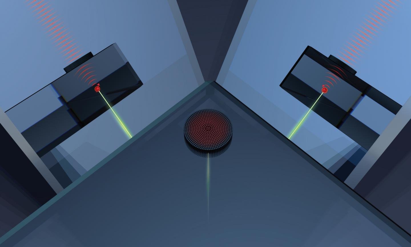
By finding a certain kind of defect inside a block of diamond and fashioning a pattern of nanoscale pillars on the surface above it, the researchers can control the shape of individual photons emitted by the defect. Because those photons carry information about the spin state of an electron, such a system could be used as the basis for compact quantum technologies. Courtesy of Ann Sizemore Blevins.
“We used the concept of a metasurface to design and fabricate a structure on the surface of diamond that acts like a lens to collect photons from a single qubit in diamond and direct them into an optical fiber, whereas previously this required a large, free-space optical microscope,” professor Lee Bassett said.
‘Right now ... the diamond NV center is simply the best platform around for room-temperature quantum information processing. It is also a leading candidate for building large-scale quantum communication networks.’
Lee Bassett, assistant professor, Dept. of Electrical and Systems Engineering, University of Pennsylvania
The metalens consists of a field of pillars, each 1 µm tall and 100 to 250 nm in diameter. The pillars are arranged in such a way that they focus light like a traditional curved lens. The actual metalens is about 30 µm across. It is etched onto the surface of the diamond and aligned with one of the NV centers inside. It guides the light that represents the electron’s spin state directly into an optical fiber, streamlining the data collection process.
The metalens operates as an immersion lens to collect and collimate the emission of an individual NV center. “We decided to collimate the light from NV centers to go to an optical fiber, as it readily interfaces with other techniques that have been developed for compact fiber-optic technologies over the past decade,” researcher Tzu-Yung Huang said. “The compatibility with other photonic structures is also important. There might be other structures that you want to put on the diamond, and our metalens doesn’t preclude those other optical enhancements.” The metalens has a numerical aperture greater than 1.0, enabling efficient fiber-coupling of quantum emitters.
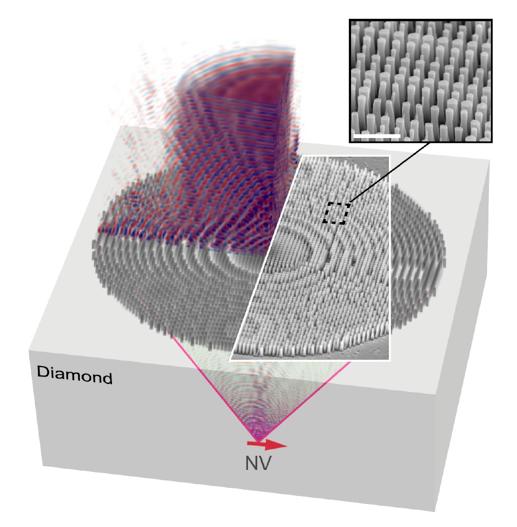
The researchers’ metalens, which consists of many small nanopillars, approximates the effect of a Fresnel lens to direct light from a diamond nitrogen-vacancy (NV) center into an optic fiber, eliminating the need for a bulky microscope. Courtesy of Nature Communications.
Nanofabrication was a key component of the project. “We needed to achieve high-resolution lithography and precise etching to fabricate an array of diamond nanopillars on length scales smaller than the wavelength of light,” Bassett said.
The flexibility afforded by metasurface engineering can provide important advantages for real-world applications of quantum technology, the team said.
“With a metastructure, we have the freedom to design any kind of profile that we want,” Huang said. “It affords us the freedom to tailor the emission pattern or the profile of a quantum emitter, like an NV center, which is not possible, or is very difficult, with free-space optics.”

(l) to (r): Tzu-Yung Huang, professor Lee Bassett, and David Hopper at work in Bassett’s Quantum Engineering Laboratory. Courtesy of the University of Pennsylvania.
This study is a step toward the team’s goal of compacting quantum technology into more efficient systems. Bassett’s lab plans to continue to explore how to best harness the quantum potential of 2D and 3D materials.“This is a first key step in our larger effort to realize compact quantum devices that do not require a roomful of electronics and free-space optical components,” he said.
The research was published in Nature Communications (https://doi.org/10.1038/s41467-019-10238-5).