New manufacturing technologies enable higher-quality displays — from big-screen TVs to smartphones — for consumer electronics.
THOMAS SCHAEFFLER, EXCELITAS TECHNOLOGIES CORP.
Consumer electronics are growing more sophisticated, at breakneck speed and with remarkable advancements in technology and refinement.
A highly visible example is the ever-increasing picture clarity in large-screen TVs, and in the evolution of smartphone products that have become essential social and productivity mobile companions to consumers in their everyday lives. A quick tour of your nearest Best Buy will introduce a dizzying array of the latest and greatest products delivering seemingly endlessly sharper resolution and increased screen size.

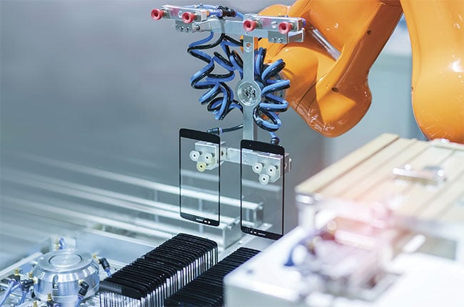
Smartphone products have become an indispensible part of our lives. There are currently around 2.5 billion smartphone users worldwide. Courtesy of Excelitas Technologies Corp.
High-tech display technology enables the development of these advanced products. Ultra-HD (UHD) televisions with 4K displays are commonly available in stores, and even higher-resolution 8K screens are coming on the market, albeit at prohibitive prices (for now). The dichotomy of product requirements between large-screen TVs and advanced smartphones (in addition to tablets, computer monitors, and so on) — and the expectation that both will offer sharp, vivid images — means manufacturing is turning to tighter and tighter tolerances. None of this would be possible without rapidly evolving inspection technologies keeping pace to detect microscopic imperfections in the submicron range.
Screen size
Televisions are designed for viewing at approximately a 9-ft distance. A modern 4K UHD screen displays 3840 pixels across the width of its surface, and the picture quality is only as good as every one of those pixels. So inspection tools are needed to detect incredibly minute defects, such as particles or dents in the surface, across an expansive 3840 × 2160 pixels.
At the other end of the spectrum, most smartphone screens are relatively small, between 4.5 and 6 in. high, with 4K resolution still uncommon. Most are currently in the HD (1920 × 1080 pixels) to 2K (2560 × 1440 pixels) range. The density of pixels is measured in pixels per inch, or ppi. The newest generation smartphones are already exceeding pixel densities of 500 ppi. Display pixels are very small, presenting their own set of quality and inspection challenges, including high-resolution inline inspection, offline inspection at submicron resolutions, and microscopic pixels that need to be closely and individually examined in the final test phases.
In addition, the newest high-end TVs and smartphones are using OLED technology for high-contrast, flexible, power-efficient displays. OLEDs are thinner, lighter, and more flexible than LEDs, and they can be made small enough for use as individual pixels, lighting up and shutting off independently of one another, and thus creating increasingly finer image contrast. However, such OLEDs require a special manufacturing step of air-tight encapsulation to achieve oxygen-free operation of the organic materials, which further presents inspection challenges.
Display panel manufacturing
A display manufacturer first produces a large master panel substrate, which is processed over several steps. Between each step, the master substrate is fully inspected to ensure that it meets quality specifications before any further processing and cost go into that panel. After it
is completely processed and passes all
inspection stages, it is then cut into smaller pieces to be integrated into the end-product device — 6 in. or smaller for smartphones, and all the way up to 80+ in. for large-format TV screens. Then additional processing steps are taken, each one followed by yet another inspection stage. In the case of an OLED display, the screen is encapsulated to prevent the organic substances from having contact with oxygen and moisture, which degrades the enhanced contrast performance and eventually results in the display’s failure. Following encapsulation of the screen, additional inspection steps are necessary to ensure the successful encapsulation of the display.
High-resolution display manufacturing is turning to tighter tolerances. This requires rapidly evolving inspection technologies to detect microscopic imperfections in the submicron range through several inspection steps. Courtesy of Excelitas Technologies Corp.
Manufacturing one display can involve dozens of individual processing steps, starting with exposure and etching in several layers to turn the substrate into a patterned panel — the so-called LTPS (low-temperature polycrystalline silicon) process. Each of these steps is validated with an inspection run. The final module tests are very different: Uniformity and brightness are measured, and the successful illumination of every pixel must be verified.
Inspection tools
While the capabilities of OLED technology create remarkable picture quality, they also challenge manufacturers’ inspection processes and tools. OLEDs’ small size requires high-resolution inspection, but it’s important to maintain short takt times. To examine each and every pixel’s quality, new inspection technology and methods are required.
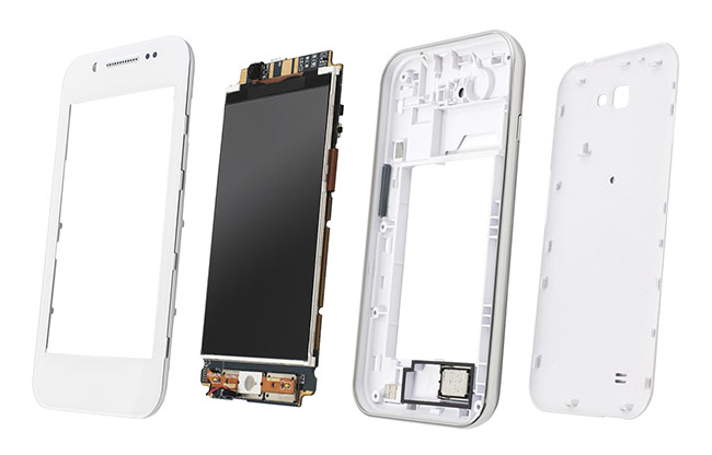
After the master panel substrate is completely processed and passes all inspection stages, it is then cut into smaller pieces to be integrated into the end-product device — 6 in. or smaller for smartphones, and all the way up to 80+ in. for large-format TVs. Courtesy of Excelitas Technologies Corp.
At each stage of manufacturing, a different approach is used for inspection. During panel manufacturing, most inspection tasks are solved with line-scan cameras, as these provide higher throughput for large areas. OLED inspection targets resolutions of a few microns for inline inspection — and even tighter tolerances for offline inspection — to detect defects well within the submicron range. Final screen tests, however, are usually carried out with area-scan cameras. These can feature up to 155 MP with very large sensors to detect imperfections in every individual pixel, among millions, regardless of which display technology is used.
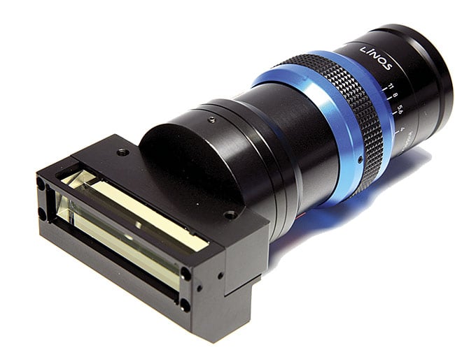
Line-scan lenses are available with a beamsplitter for coaxial illumination for inspecting highly reflective objects, such as display panel substrates, during various manufacturing phases. Courtesy of Excelitas Technologies Corp.
Quality requirements have become much stricter in recent years to avoid dead pixels and other blemishes. In fact, for reliable inspection results, the inspection camera should have several active sensor pixels for every screen pixel that is being imaged (a multiple of the resolution of
the display under examination).
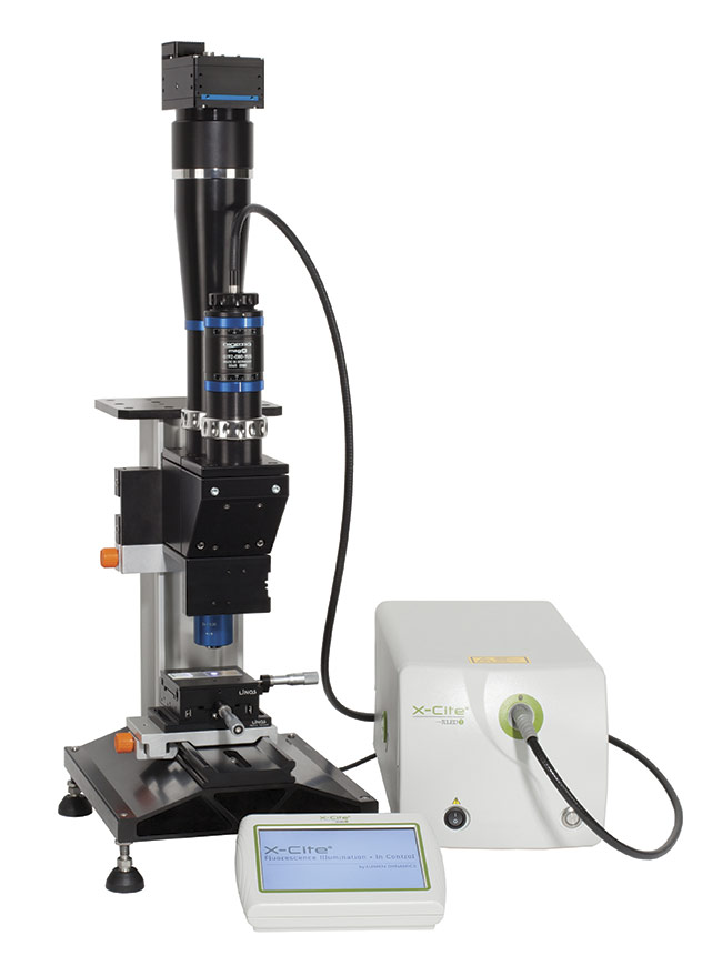
This system illustrates a highly specialized fusion between inspection optics and a microscope, enabling inspection with submicron resolution across large fields of view. Courtesy of Excelitas Technologies Corp.
Optics
An inspection camera is coupled with advanced lenses capable of sufficient magnification and resolution to allow effective inspection while also providing sufficient field of view to facilitate the fastest inspection throughput possible. OLED displays, especially AMOLED (active-matrix OLED) displays, rely on very fine structures to be able to control every individual pixel. Looking at these structures with sufficient resolution
on panels that are up to 1800 mm wide (gen 6 panels) creates a huge challenge for optics companies because the needed resolution below 1 µm is typically provided only by microscopes.
One solution is a system that fuses inspection optics with microscope technology. This type of system enables submicron resolution through large fields of view with modern line-scan sensors up to
57 mm in length, while integrating state-of-the-art coaxial illumination and autofocus.
As structures also become more complex, inspection throughput must be increased when different modes of illumination, such as dark-field and coaxial bright-field illumination, are combined. To facilitate this combination, lenses must enable coaxial illumination without sacrificing optical performance. Typically, a beamsplitter is included in the optical path to accommodate coaxial illumination.
Lenses that are not designed with a beamsplitter in the optical path generate severe aberrations if combined with a nonintegrated beamsplitter. Subsequently, the optical resolution of the inspection system will be insufficient to resolve submicron feature sizes that are prevalent in modern displays.
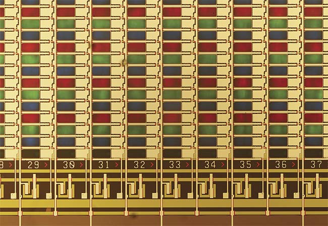
All current displays employ red, green, and blue pixels to generate a wide color gamut that includes white. When inspecting the final display, each color must be tested with the same accuracy. For the optics, this means a high degree of color correction is necessary to avoid measurement errors. Pronounced longitudinal color aberration would result in a focus shift that creates blurred images for one color, while the other two colors are in focus. Superior color correction is achieved with careful selection of different optical glasses, combined with specialized optical design. Inspection lenses must show very good color correction that enables testing of displays without the need for refocusing, regardless of what color is turned on.
Efficiency
Modern high-resolution cameras enable final tests of displays with just one camera, in one shot, whether the target is a 65-in. TV screen or a 5-in. mobile device display. Such a setup is enabled by using lenses that are optimized for the respective screen size. Optical magnification is, of course, much smaller for the big TV screen compared to the mobile display, which is imaged with a ratio of about 3:1 onto the camera sensor.
Condensing the image capture to one shot with one camera enables faster throughput than was previously possible when multiple cameras were needed to inspect numerous separate images. Using just one camera helps lower equipment costs — for cables, frame grabbers, software, and lenses — and reduces waste.
However, the optics must be able to cope with these large high-resolution cameras. For inspection purposes, the lens must show the same contrast in the center of the image as in the outer edges. To achieve this uniform optical performance, not only must every single element be meticulously fabricated to very tight tolerances, but special attention must be paid to the mounting of lenses inside the barrel as well.
Large-format lenses are often used for running final display tests with one high-resolution camera. Faster throughput helps reduce costs and is one of the contributing factors to lowering the price of these high-definition technologies. Where a 4K television might have cost $7000 a few years ago, it can be found selling in stores today for a few hundred dollars.
A display manufacturer needs the ability to produce different sizes of screens, perhaps making 55-in. screens one day and 32-in. screens the next. Flexible manufacturing and inspection solutions are therefore required. This can be accomplished without any penalty on performance by using lenses that support a large magnification range and that help minimize aberrations over a certain magnification range to adapt to the different screen sizes.
Flat panel inspection requires optics with excellent color correction for individual inspection of red, green, and blue pixels, without the need to refocus, regardless of which pixel color is active. Courtesy of Excelitas Technologies Corp.
The production of increasingly fine image quality (and more diverse sizes) demands corresponding advancements in imaging technology for inspection. As a result, the industry is challenged to continue developing optical capabilities and tools that can uphold tighter tolerances and specifications, moving display quality forward with each new product generation. Partnership and parallel innovation between manufacturing and developers of inspection technology is enabling the production of increasingly affordable high-tech gadgets that consumers want.
Meet the author
Thomas Schaeffler is head of the optical inspection business segment for Excelitas Technologies Corp. in Munich, where he leads global machine vision business and technology development to meet the needs of leading-edge inspection and machine vision customers. An 18-year veteran of the optics industry, he is also director of business technology for Qioptiq, a division of Excelitas. He has a Dipl.-Ing. (FH) degree in applied physics from Ravensburg-Weingarten University of Applied Sciences.