
Dual-Band IR Detector Can Be Integrated into Camera Chips
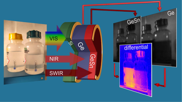
The liquids isopropanol and toluene appear transparent when viewed with the naked eye. However, when viewed in the NIR and SWIR ranges, the differences between the two become apparent, because each solvent absorbs a different amount of NIR and SWIR light. Courtesy of E. Silmola et al., “CMOS-Compatible Bias-Tunable Dual-Band Detector Based on GeSn/Ge/Si Coupled Photodiodes,” ACS Photonics, 2021, 8, 7, 2166-2173 (CC BY-NC-ND 4.0).
Scientists at the Forschungszentrum Jülich (Jülich Research Center) and the Politecnico di Milano (Polytechnic University of Milan) have developed an infrared (IR) detector that provides a bias-switchable spectral response in two distinct IR bands. When the bias voltage for the detector is reversed, the device switches from the near-infrared (NIR) to the shortwave infrared (SWIR) band. The dual-band photodetector, which is silicon (Si)-based, can be integrated into existing camera chips and smartphones.
A thin layer of Si serves as the basis for the detector; layers of semiconductor materials containing germanium (Ge) and germanium-tin (GeSn) are deposited on top of the Si layer, forming a vertical GeSn/Ge/Si stack, which is epitaxially grown on a Si wafer. The combination of Si, Ge, and Sn widens the detector’s spectral range of operation and leverages the power of Si technology.
The spectral response for the dual-band GeSn/Ge/Si detector can be tuned in the wavelength range between 1.05 and 2.45 μm (NIR-SWIR) simply by changing the bias polarity.
The detector enables voltage-tunable operation over these two optical bands at the pixel level.
Each pixel is capable of capturing the same image in different IR ranges of the spectrum. The ability to switch between NIR and SWIR, under identical illumination conditions, provides access to information that is not available from one wavelength band alone.
“In the case of paintings, for example, we can use the Ge-GeSn pixel to look through layers of paint and see how the artist composed the painting or what is underneath,” said professor Giovanni Isella of Politecnico di Milano.
The dual bands of the detector could also be used to authenticate the special inks used in banknotes that disappear when viewed under IR light.
To demonstrate the device’s ability to detect two spectral bands with the same pixel, the researchers performed a solvent detection test using isopropanol and toluene. Although both solvents appear colorless to the human eye, the dual-band detector distinguished between the two substances based on the difference in their absorption properties when viewed in the NIR and SWIR wavelengths.
Conventional Si-based camera chips can only image the SWIR range to a limited extent. Cameras made especially for SWIR imaging are typically made from materials that are difficult to integrate with standard Si circuits. “There are already other cameras that are used for these purposes,” Jülich researcher Dan Buca said. “However, their very high cost prohibits their use in daily-life application. Our detector bridges a gap, since it covers a range of the spectrum for which there have been no cost-effective sensors to date.”
It took almost 10 years for the researchers to optimize all the material parameters and designs for the device. The dual-band, IR, semiconductor-based detector that is the result of their work can be cost-effectively produced in any chip factory using established technology. Because it is Si-based, it can be integrated on existing chips with relative ease.
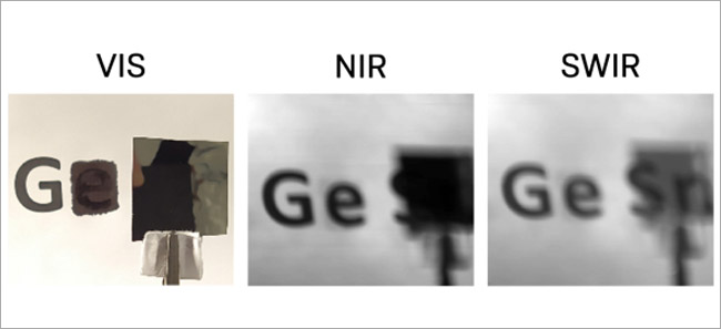
The SWIR detector developed at Jülich makes hidden letters in the NIR and SWIR ranges visible. Courtesy of Forschungszentrum Jülich/Politecnico di Milano.
“The smart combination of elements and alloys that are compatible with silicon now enables us to use a straightforward manufacturing process with standard industry tools,” Buca said. “Therefore, we are now able to construct very inexpensive camera chips that can be integrated in any smartphone just as [the chips] in visible cameras currently in use.”
The NIR and SWIR regions of the spectrum provide a wealth of information not accessible to cameras operating in the visible (VIS) range. Compared to VIS, SWIR features longer penetration depths in high scattering media, such as rain, fog, or smoke, enabling enhanced visibility in severe weather conditions and giving users the ability to estimate distance and locate obstacles. These features are important for autonomous driving, aviation, security, medical, and environmental monitoring applications.
Research leaders Buca and Isella and their respective teams will continue their collaboration, with the goal of realizing a commercial product that supports the full application potential of the dual-band NIR/SWIR detector.
The research was published in ACS Photonics (www.doi.org/10.1021/acsphotonics.1c00617).
Published: September 2021