Daniel Seiler, !%IDS Imaging%!
Worldwide energy demand is rising, and
so is the price of that energy as fossil fuel resources are consumed. These trends
have led to growing worldwide interest in alternative energy sources such as solar
photovoltaic (PV) cells. The key to success in the solar cell market, however, is
lowering their cost to manufacture by increasing production volume – and machine
vision systems are key to increased production.
A combination of technology advancements and governmental stimulus
has done just that, creating a tremendous opportunity for solar cell manufacturers.
The advancements have indeed helped lower the cost of solar PV systems while government-funded
initiatives have provided the capital for increased research and production investment.
The result is a rapidly growing market for solar cells and increased competition
to serve that market.
The appeal of solar PV systems is the abundant availability of
solar energy. Extrapolated to the whole of the Earth, this energy is equivalent to
more than 10,000 times the global annual demand for primary energy. The challenge,
of course, is to make the best possible use of this potential. The efficiency –
the amount of solar energy converted to electric power – must be as high as
possible. However, the theoretical maximum of 30 percent is far from being reached,
even under laboratory conditions, forcing the use of large solar cell arrays to
gather sufficient amounts of energy. For these large arrays to be cost-effective
energy sources, therefore, the solar cells must be as inexpensive as possible.
Solar cells usually are made of polycrystalline silicon and require
many of the same manufacturing processes as integrated circuits. There are significant
differences in their production, however. One is size: Solar cells are typically
150 x 150 mm or larger, which only high-end processor integrated chips (ICs) approach
in scale. To get acceptable fabrication yields with such large cells, the raw silicon
wafers must meet exacting demands on purity and freedom from defects.
Early detection essential
Solar cell wafers also are subject to different handling stresses
than IC wafers. The front metallization layer that forms the conductor grid on a
solar cell is applied using a silk-screen process that creates pressure stresses
on the 0.2-mm-thick wafer. This can create defects in the finished cell that can
adversely affect power production, including chipping, cracks and broken edges.
Because solar panels require many cells to work together efficiently, defects in
individual cells must be reliably identified before assembly into the panel, where
they would compromise overall panel performance.
Machine vision using high-resolution cameras is proving to be
the only viable way to ensure early detection of these defects (Figure 1). Manual
quality assurance is next to impossible because the fragile wafers are difficult
to handle. High resolution is needed because cracks as small as 120 µm long are
enough to compromise performance. The challenge is to provide such resolution at
the high throughput rate required to achieve the production efficiencies needed
to keep cell costs down.
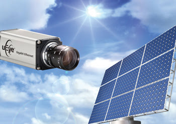
Figure 1. Machine vision systems are becoming essential tools for lowering the manufacturing
cost of solar photovoltaic power panels.
The Image Processing and Intralogistics department at Eckelmann
AG of Wiesbaden, Germany, is currently developing such an inspection station –
the E.SEE-Waferinspect – for a customer who wants to equip several wafer production
lines with the system. The system not only looks for flaws such as chips and edge
defects, but also must examine the wafer surface for contaminants, measure the wafer
dimensions to an accuracy of 50 µm and measure the angle of chamfered corners. The
production lines have a throughput of 3600 wafers per hour, leaving the machine
vision system with just under a second to complete each inspection.
To achieve the required 50-µm measurement accuracy on a 150 x
150-mm wafer, the camera needed a resolution of ~5 million pixels. Handling that
much data at the production speed required a high-speed output port on the camera
that allowed it to be positioned a large distance from the host image-processing
computer. Based on previous good experiences with camera integration, product quality,
service and support from IDS, Eckelmann decided on the UI-5480-C from IDS’
uEye series.
One camera, dual imaging
The UI-5480-C has a high-speed CMOS color sensor with 2560 x 1920
pixels and can capture and deliver full-resolution images at a rate of 15 fps. It
also offers an area-of-interest function for limiting the field of view the camera
sends to the image processor, enabling the image processor to work with a square
partial image that matches the wafer shape and eliminates distracting background.
The camera provides a Gigabit Ethernet port, supporting cable lengths up to 100
m to allow flexibility in camera positioning.
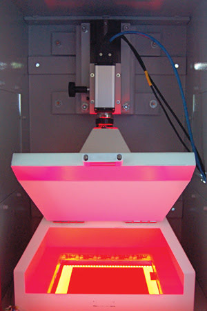
Figure 2. Dual lighting systems allow this solar cell wafer
inspection system to work with images optimized
for different inspection tasks.
To detect defects and make the needed measurements in the time
available, the inspection station takes a divide-and-conquer approach by breaking
the task into two parts. The camera is installed in a metal housing that is open
at the bottom and equipped with built-in lighting. During production, a rotary table
positions the sawn silicon wafers below the camera for in-line inspection (Figure
2). The camera acquires two successive images, each with different lighting. While
the camera is taking the second image, the image processor analyzes the first one.
The second image’s processing takes place while the station sets up for and
captures the first image of the next wafer to be inspected. Because the image capture
and analysis are performed in parallel, this solution saves valuable inspection
time.
The two types of lighting allow the processing software to work
with images optimized for different types of inspection. The first image is acquired
using diffuse red LED backlighting, which makes through-cracks readily visible.
The colored light also helps simplify the image processing used to detect and measure
the cracks. Red hides the grain boundaries on the polycrystalline silicon to prevent
the vision system from confusing them with defects. Despite the color, however,
image processing uses only gray-scale operations for speedier computation (Figure
3).
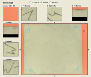
Figure 3. The red backlighting helps through-cracks to appear in high contrast to the wafer surface,
simplifying their detection using only monochrome processing.
The second image is taken using diffuse incident white LED lighting,
which provides good contrast between the normal wafer surface and any impurities
or defects. Cracks that do not pass completely through show up clearly under the
diffuse lighting. Besides detecting surface defects and contamination, the system
uses the white-light image for measuring wafer size and the chamfers at the corners.
Design for flexibility
Eckelmann’s corporate philosophy is to flexibly customize
standard components to meet the individual customer’s needs. As a result,
the E.SEE-Waferinspect system is designed to be modular so that solar cell manufacturers
can readily add other measurement functions such as grain size and wafer thickness.
An additional software module working with the white-light image measures grain
size. The addition of another camera expands on the divide-and-conquer approach
to support measurement of wafer thickness.
When the inspection station is completed, the company will have
put more than two man-years of development into camera control and image processing.
Thus, a key element supporting Eckelmann’s development of the inspection system
was the software support that came with the IDS uEye camera. The camera’s
software development kit (SDK) provided a ready-to-go interface for the image-processing
software library used in the wafer inspection system, greatly facilitating the integration
of the camera with the analysis program. Besides providing interfaces for ActiveX,
DirectShow and various libraries, the uEye SDK also features a direct programming
interface (API) for accessing drivers in C++, C# and VB.
Eckelmann’s E.SEE-Waferinspect system demonstrates only
one role for machine vision in solar cell manufacture: finished wafer inspection.
Many other opportunities exist. Machine vision can speed incoming wafer inspection,
surface treatment during processing, application of metallization and final test
of assembled panels. By speeding production and catching defects early to avoid
waste and rework, machine vision is helping solar PV systems fulfill their promise
of providing a cost-effective, renewable energy resource.
Meet the author
Daniel Seiler is a member of the marketing department at IDS Imaging
in Obersulm, Germany; e-mail: [email protected].