
Dynamically Tunable Pixels Give the Future of Displays a Refresh
Dynamically tunable pixel technology is streamlining the design and manufacture of micro-LEDs, promising new opportunities for next-generation displays.
TONGTONG ZHU, POROTECH
Considering that the average American spends over seven hours a day looking at screens, it is no wonder that the global display industry was worth a staggering $168.4 billion last year. Thanks to the emergence of wearable technology and the largely untapped potential of artificial and virtual reality (AR/VR), the industry is forecasted to grow to $297 billion by 2030.
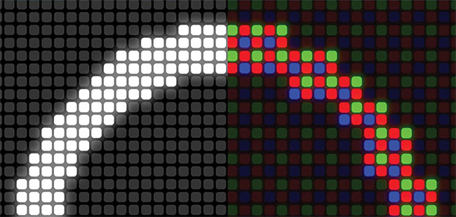
Recent developments in porous gallium nitride have led to the emergence of dynamically tunable pixels. Such tunability allows any pixel to emit wavelengths from blue to infrared and even to emit white light. Different display pixels leverage different material technologies, which complicates display manufacture and introduces performance issues. By fabricating all LEDs from the same material technology, display suppliers can allow customers to decide which color they need by driving the
LED with the proper current. Courtesy of Porotech.
But these exciting new technologies have created new challenges for the industry. The high costs, low resolutions, and bulky form factors of AR/VR headsets have prevented AR/VR technology from being swept up by the masses, in large part due to the lack of a suitable display solution.
The filtering, diffusion, and modulation stages of traditional liquid crystal
displays impose limits on how lightweight the final display can be. Similarly, emissive display technologies create stumbling blocks because they require combining light-emitting devices based on different material structures, which can also cause bulky displays.
Significant challenges exist for engin-
eers trying to solve these problems, including the funding paradox that creates a barrier of entry for new players. Funding is incredibly difficult to acquire without demonstrating a proof of concept, but developing and manufacturing such proofs and prototypes can be extremely expensive. Nevertheless, companies from small startups to some of the largest tech companies in the world are investing vast amounts of capital to find a solution to improve display designs.
Micro-LEDs manufacture roadblocks
Micro-LEDs are undoubtedly driving the next generation of innovative display technologies. In comparison to incumbent LCD, LED, mini-LED, and OLED technology, micro-LEDs offer superior brightness, high contrast, and unparalleled efficiency, as well as a longer lifetime and increased stability.
However, conventional manufacturing methods for micro-LEDs pose further challenges for the display industry.
Traditional full-color micro-LED displays, for example, use separate red, green, and blue subpixels arranged side by side on the same carrier substrate. The subpixels are typically arranged in sequences of four, comprising two red, one blue, and one green.
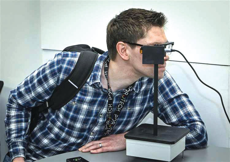
An augmented reality demonstration based on dynamically tunable pixels. The emerging pixel technology shows promise for improving the costs, resolution, and bulky form factors of AR/VR headsets. Courtesy of Porotech.
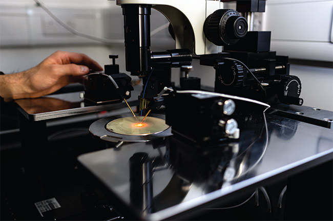
Dynamic pixel-tuning technology can now achieve full-color emission at the wafer level. It allows adjustments to both the drive current and pulse width of micro-LEDs to control their luminance and color. Courtesy of Porotech.
The red, green, and blue emitters can be independently modulated, enabling a simple, lightweight display concept that is capable of meeting next-generation display requirements. This architecture, however, currently makes the manufacturing process for micro-LED displays more complex and capital intensive.
Such architectures typically employ indium gallium nitride (InGaN) for highly efficient blue and green emitters, while the red LEDs are based on aluminum indium gallium phosphide (AlInGaP). Red InGaN-based micro-LEDs are difficult to achieve, requiring display manufacturers to mix red AlInGaP micro-LEDs with blue and green InGaN micro-LEDs on the same substrate to achieve full-color displays.
Before this can happen, each wafer must undergo a series of patterning, etching, and metallization steps to create the diode structure that will emit light when a current passes through it. However, the device characteristics and emission wavelengths of the individual micro-LEDs can vary a lot at different locations on the wafer, meaning wafers must be carefully tested so that micro-LEDs with similar characteristics can be placed in the same bin. This is an important step toward achieving the uniform image that most displays and devices require.
Such a complex mixed-material approach to micro-LED manufacture presents a major barrier to the widespread adoption of displays targeting next-generation technologies. Aside from the complexities involved with incorporating a different material for red subpixels, AlInGaP LEDs also suffer a comparatively severe drop in efficiency as the device size decreases. This limits their ability to meet both the performance and pixel-size requirements for applications such as AR/VR. AlInGaP is also more sensitive to temperature than InGaN,
adding further complications and
expenses to final display designs.
Attempts to develop red LEDs from InGaN require adding more indium to the thin epitaxial layer. This, in turn, creates an excessive strain between the InGaN epilayer and the underlying substrate — usually sapphire or silicon. Strain creates defects, which greatly lowers the efficiency, light output, and the lifetime of red LEDs made from InGaN.
The high production costs for micro-LEDs are further exacerbated by the requirement to mix multiple material
systems over micron-length scales. This has necessitated the development of
complex and expensive mass transfer technologies to position individual red, green, and blue chips in the desired pixel design. The mass transfer process naturally yields significant waste and drives up the cost of production.
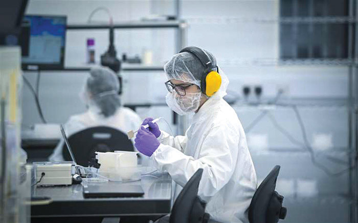
The current mixed-material approach to micro-LED manufacture not only complicates the manufacture of displays based on the technology but it also affects the lifetime performance of the displays. By leveraging the same material gallium nitride platform to fabricate red, green, and blue pixels, display manufacturers could greatly simplify the manufacture of next-generation displays and accelerate their adoption. Courtesy of Porotech.
Despite the enormous development efforts and investments going into micro-LED technology, consumer products leveraging the devices have not yet made it into the real world. Much of the problem stems from the challenges around adapting the technology to the traditional red-green-blue (RGB) subpixel approach used in conventional LED displays. But the disparate materials required to make red, green, and blue emitters, as well as the mismatched temperature performance and stability of micro-LEDs, presents further problems from a performance design perspective. Electronic compensation schemes can help to solve some of these challenges. But they are complex and add cost, bulk, and power consumption to the final design, which also affects the product lifetime.
Solving the ‘red emission’ problem
Previous research into engineered porosity in gallium nitride (GaN) accessed new functionalities and properties for the material. Further research at the Univer-
sity of Cambridge revealed that these properties had potential value for many semiconductor-based applications. Based on this research, the team spun out
Porotech with the intention of using the discoveries to improve light extraction from LEDs. However, it was soon realized that porous GaN offered a unique solution to the red emission problem in micro-LEDs, potentially enabling emitters of every color to share a similar
material technology.
The nanoporous architecture of engineered GaN sits between the top epilayer of an InGaN stack and the substrate,
acting as a buffer or strain relief layer.
As an engineered subsurface porous layer, its voids can absorb indium atoms without expanding the crystalline structure.
These voids allow indium to be added without creating the strain and defects associated with conventional InGaN epiwafers.
As a result, bright and efficient red LEDs can be realized and fabricated in InGaN using industry-standard LED
processes and tools, without any addi-
tional material treatment or complex processing steps, thereby removing a key bottleneck for the display industry.
The subsurface nanoporous architecture itself is very easy to manufacture, requiring only a single-step electrochemical process that provides excellent uniformity across the wafer. Full-color LEDs of red, green, and blue can be made from one material system and in a unified toolchain for applications in larger-format screens that typically use individual red, green, and blue LEDs. Single-color micro-LED devices on silicon CMOS backplanes have also been demonstrated to deliver industry-leading brightness and efficiency.
A solution for the full spectrum
Recent developments in porous GaN
technology have further enabled the
ability to dynamically tune pixels and,
in turn, allow any pixel to emit any
wavelength from blue to infrared.
In conventional LEDs, pixel color is
determined and actively tuned by the choice of material design, pixel architecture, and the specific driving scheme or conditions applied. By using the same underlying concept enabling red micro-LEDs, dynamic pixel tuning technology can now achieve full-color emission at the wafer level. It allows adjustments to both the pulse height (drive current) and the pulse width to control luminance (brightness) and color. This enables a single micro-LED chip to produce any visible color from a single pixel, including white light. It removes the need to have RGB subpixels and dedicated drive circuitry for each color, as well as the physical space that is required to lay subpixels side by side.
Dynamic pixel tuning carries the potential to shift display manufacturing from the constraints of the conventional RGB pixel format, to greatly enhance design and commercial flexibility for LED device-makers. By fabricating all LEDs from the same material technology, display suppliers can allow customers to decide which color they need by driving the LED with the proper current.
The impact on displays
The move away from RGB pixels also means that displays are no longer constrained by the three primary colors. This potentially significantly expands the available range and resolution of future displays. Further, the higher-resolution displays can be produced with a substantially lower defect rate, and they use less complex manufacturing processes, based on silicon carriers. This breakthrough is particularly important for small form-
factor displays that demand high resolutions, such as AR/VR displays, as well
as wearable technologies.
Because dynamically tunable pixels can change color, they eliminate the tricky color-conversion step of conventional fabrication methods. This elimination is significant because perfecting this process is one of the major challenges within the micro-LED industry. Removing this step also leads to improved process yield and reduced costs.
In addition to the manufacturing benefits that dynamically tunable pixels
provide, the technology also opens up new options in system-level design, the most significant of which is the option
to trade resolution for brightness and
efficiency. Replacing four RGB full-color pixels with a single, larger, dynamically tuned pixel maintains the full-color resolution of the microdisplay and offers a significant advantage in terms of brightness and efficiency. As the size of a micro-LED gets smaller, the edges of the device represent a larger percentage of the device area. The edges of the micro-LED are where most of the defects occur that reduce device efficiency and light output. Replacing a trio of RGB micro-LEDs with a single, larger, dynamically tunable pixel reduces the ratio of the edge area to the emitting area, thus allowing a more efficient and brighter LED.
Making micro-LED displays a reality
Such breakthroughs in porous GaN and dynamically tunable pixels enable
production of all three light-emitting
elements using a single toolchain,
removing the complexity and expense of fabricating displays by mixing devices based on different material structures. By eliminating the need for mass transfer
manufacturing methods, this new technology also reduces the costly waste involved in micro-LED production, while improving yields. Currently, dynamically
tunable pixel architectures are being fabricated on 8-in. silicon substrates, with plans to move the technology to 12-in. silicon wafers. The larger substrates allow more devices to be processed at once — compared to typical 4-in. or 6-in. sapphire substrates — taking advantage of economies of scale.
This positions dynamically tunable pixel technology as a supply chain-ready solution that addresses the system integration and engineering issues needed to realize an all-in-one micro-LED. The overall process massively simplifies display manufacture, while offering better performance and design freedom for the entire optical system.
Barriers remain in achieving the scale required to realize some of the economies
involved with dynamically tunable pixels. The vastness of the semiconductor industry and its disparate nature mean that each individual player must work and collaborate with several partners to bring each innovation to the market. Forging partnerships and securing a fab slot is both a lengthy and a costly process.
But the technology is on course to change the future of micro-LED displays. Access to the right resources and partners will guide how quickly the industry is able to position the technology for commercialization. The all-in-one pixels will consign RGB to the past. They will introduce improvements in display resolution, color, brightness, and efficiency, and they will ultimately expand manufacturing options and design latitudes for consumer technologies such as AR/VR.
Meet the author
Tongtong Zhu, Ph.D., is CEO and co-founder of Porotech. He has a background in physics,
electronics, engineering, and materials
science, as well as over 15 years of experience with III-nitride semiconductor materials.
His vision is to champion micro-LED
innovations for global market adoption;
[email protected].
/Buyers_Guide/Porotech/c33159