2022 saw war break out in Europe, supply chains strained by the everlasting pandemic, and, just this month, a long-anticipated breakthrough in laser fusion making global headlines and raising hopes for the future prospect of green energy. And the laser industry? Read on.
For the last few years, I have taken time in December to reflect on what happened in the last year and what it means for the one to come. I would reflect on the major events within the laser industry and sometimes speak with key people to learn what interesting perspective I might find.
It is impossible to proceed with a discussion about 2022 without a word on Russia’s war in Ukraine, which continues to shock the global community with its brutal and senseless waste of human lives. The pandemic was another catastrophe, although perception of its relative threat has changed over the year. Even China has finally given up on its “zero-Covid” policy, which placed strong limitations not only on everyday life in China, but also on essential business activities. Western businesses that tried to send service engineers to China will greet the news with relief.
But how has the laser industry fared? Here in Germany, the privately held TRUMPF group reported a robust 20% increase in revenues for its financial year, which ended in June. TRUMPF also saw a whopping increase of 42% in orders.
U.S.-based Coherent Corp. (formerly known as II-VI Inc.) posted a 7% increase in revenues and a 29% increase in bookings, as disclosed in its annual report.
The industrial laser market expands
In a recent talk with laser market analyst Dr. Arnold Mayer, he shared a bit more about the bigger picture for the laser sector. “I expect the global market for industrial laser systems to reach $22 billion in 2022, unchanged versus 2021,” Mayer said. “While demand in the Americas showed robust growth, it decreased in China, which is the largest market. Demand in Europe grew in local currencies, but the dollar value did not increase due to the large exchange rate shift.”
Asked for his thoughts about next year, Mayer added, “For 2023 I expect growth in the range of 5% to 10%. Visibility is especially low due to the uncertainties weighing on the market trend in China.”
Expect cutting and welding to make up the biggest portion of the market, with increased demand for laser and optical systems from the semiconductor sector.
New foundries everywhere
Following the passage of the U.S. CHIPS and Science Act, a number of new semiconductors fabs are planned for construction — a trend likely to last for years thanks to the $52 billion apportioned by the U.S. Congress to support its domestic chips sector. TSMC alone is supposed to spend $40 billion for chip facilities in the US. Intel, GlobalFoundries, Samsung, Texas Instruments, and others have also shared plans to join the pack with their own U.S.-based fabs in an investment spree that is already on track to exceed $200 billion.
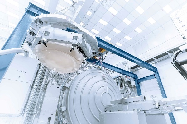
Optics supplier Zeiss SMT built a garage-size vacuum chamber for metrology of the optics used inside ASML’s high-NA EUV lithography machines. Courtesy of ZEISS SMT.
And momentum is building elsewhere. Reuters recently reported that China’s government is preparing a 1 trillion yuan ($143 billion) package to boost its own domestic semiconductor industry, and Europe also has its own version of the CHIPS Act in the works, only with less juice. Nevertheless, Intel announced plans to build a huge chip-making facility in Magdeburg, Germany, two hours west of Berlin. The German government has allocated €6.8 billion for the project already.
All of these efforts will contribute to long-term growth in photonic capital equipment targeting the chips sector.
Will that meet current market demand? Peter Wennink, CEO of technology leader ASML, shared a number of interesting facts at the company’s investor day this year. Among them is his expectation for an annual growth rate of around 9% for the semiconductor market, and a doubling of semiconductor revenue between 2020 and 2030.
Keeping Moore’s law on track
Good news is coming from the technology side, too. Extreme ultraviolet (EUV) lithography has been the recent technology driver in lithography. Like others, I’ve long wondered what could be done to achieve even smaller structures on chips. Now we have the answer: EUV with a larger numerical aperture (NA). Personally, I have long wondered what equipment-makers could do to extend or replace EUV to produce even smaller features on chips. Well, the answer is … EUV with a higher numerical aperture (NA). In short, a higher NA means that larger mirrors project patterns onto the chips, enabling smaller structures. There is no technology published beyond high NA EUV, but this technology will last at least until 2030.
Supply chain problems should lessen
For the last two years, supply chain issues have substantially hindered the production of laser systems and other photonic manufacturing equipment and end products.
One laser supplier told me this month that his company had to promote an older system because it couldn’t get all the parts for the new generation of products. Another supplier, who spoke to me despite being sick at home, said, “Supply chain issues are just like my cold. I hope it will be gone in the new year.”
These comments probably reflect how many industry people think about the supply chain disruptions. Risks continue, but there is room for hope.
Filling jobs a challenge
Hope is certainly not the solution for another problem plaguing the photonics industry: finding qualified workers.
Berlin-based Scansonic MI GmbH recently lost a few people to the nearby Tesla factory, and, according to Axel Luft, managing director of the Berlin-based Scansonic MI GmbH, the company has turned to personal contacts or headhunters to fill the gap. Another German company, TOPTICA Photonics, employs a total of 450 employees around the world; it lists 50 vacant positions on its website.
The challenge of filling photonics jobs is a bit different in the U.S., where big tech companies like Meta and Intel announced big layoffs this year.
The workforce disruption from those layoffs came quickly, and it was disorienting, Tom Hausken, Optica’s senior industry adviser, told me from California, “The employment data is still good, and there are still open positions across the economy, including in our industry,” he added. “It should mean that the employers who were struggling to fill positions before — such as many small companies, large military contractors, and government labs — will finally be able to fill more of their needs.” That applies to hot job sectors like quantum technology as well as for more conventional optics and photonics engineering.
Fusion and flight
Readers no doubt expect laser fusion to be a big part of this 2022 roundup. I am a big fan of laser fusion. I visited NIF in January 2022 and I was deeply impressed. It is a journey that every laser nerd should do once in his or her life. It is also obvious that the recent results reported by NIF are tremendous, and Photonics Media is tracking new developments closely. All of that said, I do not see fusion contributing to the energy problems we face within the next 10 years.
A topic that I expect to be much more immediately relevant for photonics markets in 2023 is a few hundred miles (or kilometers) above our heads: low-Earth-orbit satellites. The next generation of satellite constellations will use laser terminals for free space communication. And that trend will create revenue of several hundred million dollars for photonic components from launch. Each of those satellites will need four such terminals, with a unit price in the six-digit region.
RIVADA Space Networks, for example, plans to launch 300 satellites in 2025. All of them will carry four laser terminals for a total of 1200.
“Laser terminals communicate directly, there is no need for ground-based gateways anymore. And they are now available from several sources,” said Thomas Laurent, director of business development at RIVADA.
After an evaluation by DARPA, the American Space Development Agency announced that the National Defense Space Architecture, with several hundred satellites, will use optical communication terminals as well. If other satellite fleets pick up the new technology — and I predict they will — the technology could quickly grow to a billion-dollar market segment for photonic components.
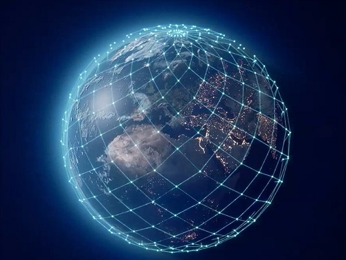
Laser-linked satellite networks launched into low Earth orbits will create a major new market segment for optical components within the next three years. Courtesy of RIVADA Space Networks.
Laser countermeasures deploy
There is another trend related to defense: high-energy laser weapons. Right after the invention of the laser, the expectations were high that lasers would be the biggest breakthrough in the weapons area since the atomic bomb. Funding budgets worth millions of dollars were allocated.
Fifty years later, the laser is more active on the battlefield. Israeli company Rafael Advanced Defense Systems, for example, offers the 7.5-kW LITE Beam laser system to counter small drones at distances up to 2 km. Rafael labels a larger version employing a 100-kW “Iron Beam,” and it is similar to the company’s Iron Dome system, which has intercepted more than 2500 rockets already. The sales argument for the laser is its low cost per shot, which according to a video from The Wall Street Journal, is $2 per laser shot — a remarkable contrast to the $50,000 cost for each of the Iron Dome’s interceptor missiles. The same video shows the limitation: The laser is heavily dependent on a clear line of sight. Any fog, rain or snow makes it ineffective. In other words: Such a laser system will never be a stand-alone solution.
Still, President Biden has promised support for both the Iron Dome and Laser Dome systems. And just recently, U.S. weapon-maker Lockheed Martin announced a cooperation with Rafael to develop a laser weapon system that could be market-ready next year. So, six decades after the invention of the laser, deployment of the technology in defense countermeasures is finally poised to accelerate.
Being present
Discussing future weapons platforms is no way to close a holiday post. Fortunately, as this writer was looking for a suitable conclusion, his son came in to remind him that it was time to go find a Christmas tree. It was already dark outside with a little bit of snow covering the roads, and very cold — too cold for walking outside, according to the boy. But when we found the most beautiful tree ever, he was happy and we brought our precious conquest home. So, it is time to be present and prepare for the holiday season. The new year is coming soon, and there is good reason to expect it to be better than the old one.