
Existing Fab Methods Could Yield ‘Light Prison’
A “prison for light” designed by Dutch theorists could be created using existing silicon-etching techniques and play a role in optical communications.
The inverse woodpile photonic crystal has an atomic structure similar to diamond and incorporates arrays of perpendicular pores. One pore in each set has a smaller diameter, forming a point-defect at their intersection where light is confined.
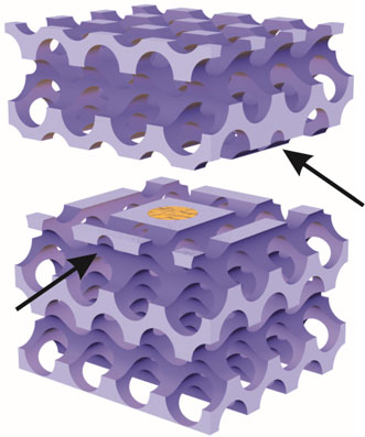
The photonic bandgap crystal has a diamond-like structure, made of two sets of mutually perpendicular pores drilled in silicon. To realize a resonant cavity, one pore in each set (indicated by black arrows) has a smaller diameter. At the intersection of these two pores, a point-defect appears capable of confining light appears. Courtesy of MESA+.
The crystal would have a record-wide photonic bandgap, according to its designers at the MESA+ Institute for Nanotechnology at the University of Twente. Up to five isolated and dispersionless bands appear within the bandgap, with wavelength ranges compatible with telecommunication windows in the near-infrared.
The mode volume of the cavity resonance is as small as 0.8 λ3, indicating a strong confinement of the light, the researchers said.
Confining photons has many applications in optics, such as efficient miniature lasers and LEDs, as well as on-chip data storage and biosensors.
Previously, the team showed that diamond-like photonic bandgap crystals can be etched in silicon, with techniques commonly used in CMOS fabrication. The new cavity design could be applied during the routine fabrication of photonic crystals, they said, opening the possibility of integrating ultrafast photon manipulation with existing electronic information manipulation.
The work was published in Physical Review B (doi: 10.1103/PhysRevB.90.115140).
For more information, visit www.utwente.nl.
Published: September 2014