While F2 lasers await their entrance into the microchip manufacturing market, they're perfecting their chops in spectroscopy, optics characterization and micromachining.
Daniel C. McCarthy, Senior Editor
Compared with other excimers, F2 lasers emitting at 157 nm have few commercial applications. In fact, were it not for microlithography, it’s possible that these excimers would remain laboratory curiosities for years to come.
As it is, their largest market is still three years distant, when the semiconductor industry plans to roll out F2-equipped steppers. But laser suppliers aren’t waiting until then to distribute 157-nm sources designed for smaller markets. In two or three years, chip manufacturers will apply F2 technology refined by applications in spectroscopy, optics characterization and micromachining.
Of these niche applications, scientific users represent the largest share, with 60 percent of the nonlithography market, according to Rainer Paetzel, product manager for Lambda Physik in Göttingen, Germany. Spectroscopy — academic and industrial — underlies most of these applications.
Characterization of optics and coatings is next, with 30 percent of the market. Many of the applications in this segment are driven by developers of 157-nm lithography.
Three years from now, the semiconductor industry will begin implementing
157-nm excimer lasers to produce 70-nm critical dimensions on chips. In
the meantime, the high 7.9-eV energy of 157-nm photons is enabling
micromachining capabilities impossible with longer-wavelength lasers.
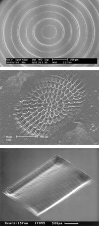
The wavelength is particularly effective in machining quartz, as shown
by the microlens structure (top), and in producing complex patternbs in fused silica (bottom) and PTFE (middle). Image of the microlens structure courtesy of Laser Zentrum Hannover. Other images courtesy of Lambda Physik.
The smallest piece of the pie goes to cutting-edge micromachining applications, which would normally be defined as an industrial usage except that most work in this field remains in the laboratory.
Scientific and industrial research may be the only application, besides microlithography, that could support an F2 laser market. One reason is that 157-nm photons deliver a 7.9-eV quantum energy to the target, eliciting interaction cross sections that are higher by several orders of magnitude than longer wavelengths. In other words, they can photo-ionize and photodesorb sample materials in a single step, particularly transition metal atoms and complexes.
The lasers, for example, enabled professor H. Floyd Davis’ chemistry group at Cornell University in Ithaca, N.Y., to study reaction dynamics among small molecules and ground state and electronically excited transition metal atoms and complexes.
Another reason why research is the largest nonlithography market for F2 lasers may be that, compared with other applications, it does not depend as much on specialized beam parameters, making F2 lasers more economically feasible. In fact, repetition rate — one of the most important parameters elsewhere — is limited in spectroscopy by the prevalent data acquisition technology, which often is in the hertz range. Many excimers measure data repetition rates in kilohertz.
The beam parameters important to spectroscopy are fluence and pulse-to-pulse and spatial stability, said Heinz Huber, sales and marketing director for TuiLaser AG in Munich, Germany.
“[Pulse energies] on the order of 1 mJ are very comfortable,” he said. “You want a reasonably high number of photons to give you a concentrated number of ions you can comfortably count.”
Pulse-to-pulse stability, which should have less than 2 percent variation, improves signal-to-noise ratio and helps simplify averaging of results. Spatial stability on the order of 100 μrad enables illumination of the material with constant energy density, sustaining reproducible experiments.
F2 lasers are low on the list of challenges that the semiconductor industry is confronting on its road to 70 nm. The same can’t be said for the beam delivery systems, which will rely more on CaF2 lens materials than current steppers do. The new design and manufacturing issues that these optics present require intensive characterization and metrology efforts to keep the semiconductor industry on track.
What better tool to characterize 157-nm optics than 157-nm lasers?
F2 lasers that are used to characterize lithography lenses, however, need not be as sophisticated as those that will drive lithography steppers. In fact, most suppliers to this market exchange power for size to deliver less expensive instruments that can fit on a laboratory benchtop.
“For metrology of lens elements, you’re using interferometric methods,” Paetzel said. “You pick up a small portion of light, but you need lots of pulses to average your signal. The energy per pulse doesn’t do you any good, so you want low energy.”
Spatial stability is always what you want in inspection, Huber added. “What people are doing is ... sensing variations from the standard to a fraction of a percent. So it must be imaged homogeneously.”
The spatial beam profile should have a flat top. If you take 80 percent of the central beam, you should get ±5 percent homogeneity, he said.
Micromachining, the smallest nonlithography market segment for F2 lasers, is also the most specialized, so the instruments tend to be more expensive. This partly explains the technology’s comparatively small market penetration.
The 157-nm wavelength narrows the resolution with which to drill microvias and pattern features, and its high-energy photons couple strongly with fused silica and quartz as well as with weakly absorbing polymers such as polyethylene and PTFE.
Despite the potential of F2 laser technology, none of the contract machining houses contacted had implemented these sources, nor had they heard of anyone using them for commercial machining.
“We need to take a pragmatic point of view from the manufacturer’s perspective,” explained David Wall, director of sales at Resonetics in Nashua, N.H. “If we can meet our customer’s specifications and quality characteristics at 248, then it makes more sense to do that. If necessary, we can go to 193 because we can’t quite get what we need at 248 nm, in which case we’ll establish a manufacturing model for 193.”
In other words, the tolerances and the economics of machining with 157-nm radiation haven’t yet intersected to form a commercial market. But researchers at the University of Toronto are exploring its potential in collaboration with the Laser Labora?torium and MicroLas Laser?system GmbH, both in Göttingen.
The researchers configured a cylindrical lens system to homogenize the beam from a Lambda Physik LPF 220i F2 laser and to focus it on a 6 x 6-mm aperture for uniform illumination at the mask plane. A 25x Schwarzschild lens delivered uniform ±5 percent on-target fluence of 6 J/cm2 in a 0.25 mm x 0.25-mm field.
The system extends the possibilities for fabricating grating phase masks, high-aspect-ratio vias, rib waveguides and other optical components. For example, the group was able to excise parallel trenches in an 8-μm-thick layer of germanosilicate deposited on a 20-μm-thick silica substrate. The light-guiding ribs between the trenches measured 8 μm wide and 4 μm high and had edge resolution of 2 μm.
Peak power density is one of the most important laser parameters for materials processing, depending on the application. Lower densities may simply modify the material, while high densities of 157-nm radiation dissociate molecules and ablate it.
Power density varies, depending on where along the beam it is measured. Beam divergence distributes energy unevenly.
Obviously, focusing beam energy into a tighter spot can help increase peak power density. But another way is to increase peak power by shortening the pulse length. Shorter pulses also improve energy efficiency. At high fluences, most of the work happens in the first 5 ns. The beam will continue to ablate material after that period, but it is impeded by a phenomenon called plasma shielding. The effect is caused when laser-induced plasma ignites over the target area, essentially obstructing radiation from the surface.
That suggests, at certain power densities, that a 10-ns pulse can ablate as quickly as a 20-ns pulse, but with 30 percent less energy, Huber said. “Therefore, the more energy you can deposit before that 5-ns limit, the better ablation rate,” he added.
As in lithography, repetition rates are important to the throughput and consistency in small-area processing. The total required energy is best distributed among several low-energy pulses rather than in a single high-energy pulse. Faster pulses, however, dilute a laser’s fixed energy per pulse over time: Average output power is calculated from the energy per pulse and the repetition rate divided by 1000. Higher output powers, therefore, enable higher repetition rates without compromising a laser’s average power output.