Microlens arrays manufactured using polymer injection molding and a highly precise micro-cutting process are ideally suited for LEDs, smartphones and consumer electronics.
OLAF KRAFT, JENOPTIK POLYMER SYSTEMS GMBH
Polymer optics are one of the cornerstones of photonics, driving the innovation necessary to meet the requirements for ever-smaller installation spaces and significant weight savings, all while achieving a higher image quality. The miniaturization of optics using micro-structured surfaces today can be found in many areas including smartphones, LED lighting and consumer electronics, where these attributes are particularly important.
Compared to glass-based optics fabricated using traditional manufacturing methods, there are numerous advantages of polymer-based optics manufactured by ultraprecision technology and injection molding processes. Efficient production processes and fully automated manufacturing have meant abundant supplies of inexpensive, low-density polymers. Another advantage: Polymer optics afford a much greater degree of freedom in design than glass optics.
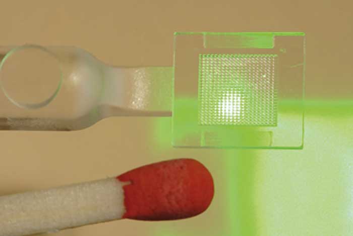
Microlens arrays are highly versatile and can be found in numerous everyday applications. Courtesy of Jenoptik GmbH.
One of the best examples of miniaturized and versatile polymer optics is found in microlens arrays. Used for refractive or diffractive beam homogenization, microlens arrays are incorporated in light-mixing rods or honeycomb condensers for projections and homogeneous illumination.
The periodic arrangement of a number of microlenses is described by the “pitch,” measured from its center-to-center distance and combined to refer to a single microlens array. These require exceptional dimensional accuracy and reliability. The geometry of the lens arrays is typically spherical or cylindrical with a regular or hexagonal arrangement. In order to understand the future boundaries and challenges of high-quality microlens arrays and their fabrication, it is important to first consider the traditional production methods in conventional micro-optics.
Grayscale lithography
One of these traditional micro-optics fabrication methods is grayscale lithography, in which a complex surface topography is generated in a photoresist in a single exposure step. For this purpose, a photoresist is typically spun onto a transparent glass substrate in the desired thickness through a process called spin coating. Next, the resist is exposed using a laser beam, an electron beam or illumination through a grayscale mask. The exposure dose is varied locally and a different solubility of the photoresist is achieved for a specific developer. If a laser or electron beam is used, the local differences can be produced by altering the exposure time, the beam energy or multiple exposures. If a grayscale mask is used for the exposure, the dose is varied by a local change in the mask transmission. Fabricating microlens arrays in lacquer or ultraviolet adhesives requires several steps and is therefore very labor intensive. The result may be measured using an interferometer.
Both binary pseudo-grayscale masks and conventional grayscale masks can be used. Pseudo-grayscale masks have a chromium layer with a multiplicity of binary structures of various densities, all with a diameter less than the wavelength of light. These structures represent chromium-free spots in the otherwise opaque layer. When these masks are illuminated, only a moderate light transmission is achieved and the light is not refracted because of the very small structures.
In contrast, conventional grayscale masks have locally different degrees of transmission as a result of absorption. These local differences in transmission are achieved by exposing a high-energy, beam-sensitive glass mask to an electron beam or a laser direct-write glass mask to a laser beam1,2.
The subsequent nonlinear development process must be taken into account in the exposure of the photoresist by grayscale lithography. After the development of the resist, the structure can be transferred onto a glass substrate by a further dry etching process. Resolutions of approximately 0.5 µm can be achieved with grayscale lithography. Microlens arrays with high fill factors are possible, though depths are generally only a few tens of micrometers.
Thermal reflow processes
Thermal reflow processes for fabricating microlens arrays utilize a binary-structured resist layer for the generation of the arrays. As with grayscale lithography, the first step is to spin a thin layer of resist on a carrier substrate. The resist can be structured by exposure with a binary mask, an electron or laser beam. Once the photoresist has been developed, binary regions with the aperture diameter of the microlenses remain. Subsequent heating of the resist layer above the softening point results, due to surface tension, in the formation of an almost spherical boundary surface for each lens. The structure is then transferred onto a glass substrate in a final dry etching step. Once again, as a result of the multiple manufacturing and heating processes, this is a labor-intensive method of producing structures and contours3,4.
A thermal reflow process can be combined with the grayscale lithography described earlier. In this case, after melting, the resist is again exposed locally with different exposure doses in order to produce aspherical surfaces. If no additional exposure is applied using grayscale lithography, the surface shapes and radii that can be achieved will be limited by the surface tension, the thickness of the resist layer, the aperture shape of the lens, and the temperature control during the melting of the resist. Since the thermal reflow process is based on a binary resist mask, it is difficult to produce microlens arrays with a high fill factor5.
Two-photon lithography
Two-photon lithography, also known as direct laser writing, is based on two-photon absorption processes for the exposure of a photoresist. The resist is illuminated locally with a focused laser beam; for the elective wavelength, there is a low absorption of single photons. In the focal region, however, the probability of two-photon absorption increases if the light intensity of the laser is sufficiently high. This process changes the solubility of the resist for specific developers. Since the light intensity is only suitable for two-photon absorption in a small 3D region near the focus, only a small volume of resist will be exposed. This volume is referred to as the voxel. Two-photon lithography therefore makes it possible to produce 3D structures in photoresists. At the same time, this method requires 3D exposure, particularly for microlens arrays, to obtain a stable resist structure.
Two-photon polymerization is a similar process. In this case, a liquid resist is cured within a voxel using a two-photon absorption process. The method spans several process steps.
The resist structures resulting from both processes can be molded or transferred onto glass using a dry-etching process, depending on the surface. Both technologies make it possible to produce microlens arrays with continuous surfaces, high spatial resolution and steep flanks.
Ultraprecision technology
An alternative to the conventional manufacturing methods described above for miniaturized optics such as microlens arrays is the use of ultraprecision technology in the prototype phase, as well as injection molding in any subsequent series production. The combination of these technologies makes it possible to achieve extremely high levels of precision and dimensional accuracy. Furthermore, it enables the fabrication of freeform shapes, and concave and convex surfaces, at a sample cost of just a few hundred dollars.
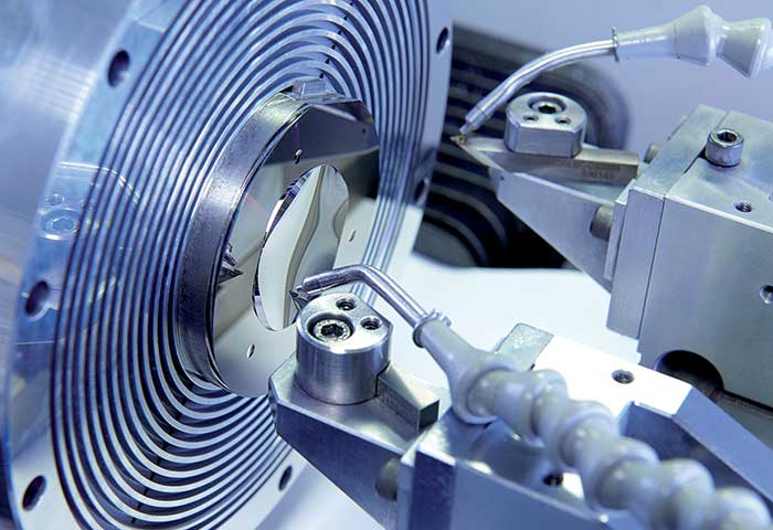
Ultraprecision machining enables the fabrication of freeform molding tools. Courtesy of Jenoptik GmbH.
Ultraprecision technology is a micro-cutting process in which high dimensional accuracies of 0.1 to 1 µm are achieved using diamond turning and ultraprecision milling. The radii of monocrystalline diamond milling tools are generally greater than 100 µm. The requirements in terms of machinery, measuring equipment, the production environment and process expertise are very high. Measurements are carried out exclusively with optical and tactile measuring systems to achieve the highest level of measuring accuracy. These surface structures are usually no longer visible to the naked eye. A special simulation program is used to ensure an optimal process design even before the machining stage. The machining equipment itself is specially designed with rotary axes with aerostatic bearings and the use of vacuum clamping technology. The spindle used for the fabrication of microlens arrays can reach up to 80,000 revolutions per minute, which is an absolute peak value, according to the current state of the art. In addition, the process environment for the machines is isolated from vibrations.
The materials machined with ultraprecision technology have traditionally been optical, thermoplastic polymers such as polycarbonates or polymethyl methacrylate. However, increasing numbers of micro-structured components with more complex structural requirements can be machined using ultraprecision technology in a wide selection of materials. Depending on the complexity and geometry, a sample can be produced in anything from a few days to a few weeks. This is particularly significant in terms of design validation, to move into series production as quickly as possible and implement changes quickly.
Ultraprecision technology has proven its worth over many years for prototypes and small-scale series production of optics, as well as for applications at the interface between optics and mechanics. In addition to microlens arrays, constant-curvature freeforms can be found in head-up displays, head-mounted displays, LED ambient lighting and cellphone spotlights.
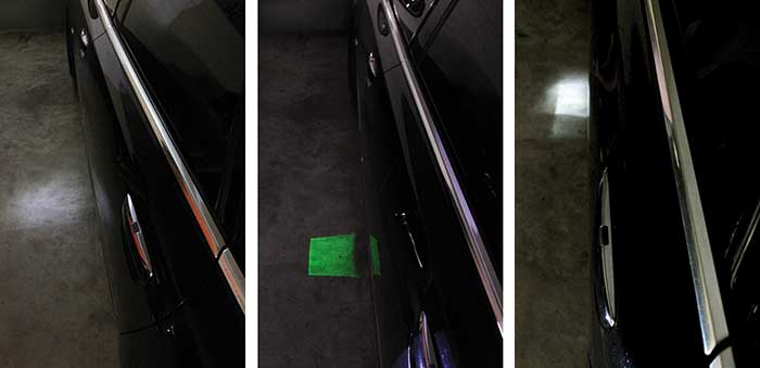
The use of microlens arrays with both LED (a) and laser light (b) sources leads to a significantly more homogeneous illumination in the automotive field than LED light sources without a microlens array (c). Courtesy of Jenoptik GmbH.
The use of microlens arrays with both laser and LED light sources leads to a significantly more homogeneous illumination, the benefits of which can be seen in the automotive and communications fields, as well as in consumer products.

The use of microlens arrays with both LED (a) and laser light (b) sources leads to a significantly more homogeneous illumination in communication fields and consumer products, such as a smartphone, than LED light sources without a microlens array (c). Courtesy of Jenoptik GmbH.
Once a sample produced using ultraprecision technology has been approved, it is transferred into series production and fabricated using injection or compression injection molding. The correct tooling concept and mold design play a decisive role in determining the price and quality.
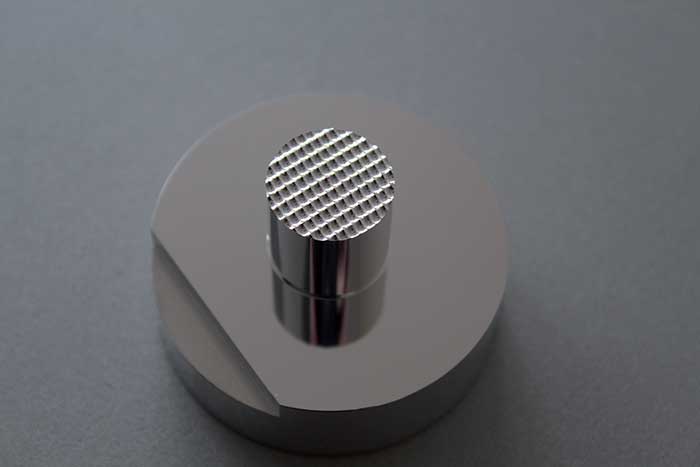
Microlens arrays that are fabricated using ultraprecision technology are characterized by their high dimensional accuracy. Courtesy of Jenoptik GmbH.
Optical quality is determined particularly by the potential for stresses in the material, which, evidence shows, is influenced by the wall thickness — the thinner the component, the higher the potential for stresses. In order to keep the stresses as low as possible, some basic rules must be observed in the mold when it comes to the geometry and position of the gating, forming pressure, changes in wall thickness, breakouts and edges.
In addition, exceptional process stability during the molding process is essential to maintain a consistently high level of precision and quality. This means a homogeneous filling process during injection molding and a defined injection speed, as well as a controlled temperature during the cooling process.
Depending on the geometry and the requirements, temperature control of the injection mold can be constant or variothermal. Shape deviations will then be in the region of peak-to-valley = 0.7 µm or root mean square = 0.3 µm. For very thin moldings such as microlens arrays, wall thicknesses of 0.2 mm can be achieved in this way.
Injection molding is ideal for large and very large unit volumes and fabrication with a high level of automation. Since a fully automated production line, including packaging and the complete handling process, can produce approximately 10 to 30 million units per year at a unit price of one to two dollars — the higher investment costs will be well worthwhile.
The combined use of ultraprecision technology and injection molding from a single source represents the optimum combination of technologies for fabricating polymer microlens arrays in large quantities that meet the highest quality requirements such as applications at a sustained maximum temperature of up to 200 °C, at a competitive cost compared to standard technologies.
This is why these optical precision parts made of polymer now dominate the market for mass-produced items.
Meet the author
Olaf Kraft, sales manager at Jenoptik Polymer Systems GmbH, has been selling optoelectronic and mechanical products for more than 25 years; e-mail: [email protected].
References
1. C. Wu and L.A. Wu (May 13, 2003). Direct Write All-Glass Photomask Blanks, U.S. Patent No. 6,562,523 B1.
2. C. Wu (February 25, 2003). Gray Scale All-Glass Photomasks, U.S. Patent No. 6,524,756.
3. Y-H. Pao and P.M. Rentzepis (1965). Laser-induced production of free radicals in organic compounds. Appl Phys Lett,
Vol. 6, p. 93
4. E.B. Kley (1997). Continuous profile writing by electron and optical lithography. Microelectron Eng, Vol. 34, Issues 3-4.
5. E. Roy et al. (2009). Microlens array fabrication by enhanced thermal reflow process: Towards efficient collection of fluorescence light from microarrays. Microelectron Eng, Vol. 86, Issue 11, pp. 2255-2261.