Flexible glass offers advantages for new applications, device designs, and fabrication processes not possible or practical with alternative substrate materials.
SEAN GARNER, CORNING RESEARCH & DEVELOPMENT CORP.
A strong driving force toward increased interaction and connectivity runs through our society. And it does not end when people put down their smartphones, tablets, or smartwatches.
The ability to enjoy constant connection to communication and information began with ubiquitous mobile consumer electronics, but this functionality is now becoming integrated on larger scales into items such as automobiles, video walls, and household appliances — namely refrigerators.
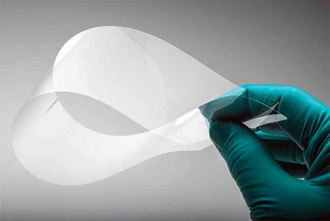
Flexible glass provides a thin, lightweight, and bendable substrate that enables new application form factors and large-scale electronic device integration. Courtesy of Corning.
Increased connectivity is no longer sought simply for interpersonal communication. The Internet of Things offers ever-increasing interactions that never existed before between objects in the environment. And as this electronic functionality migrates to new platforms and form factors, advances are needed in the underlying device technology to enable equivalent performance at these different scales and form factors.
For this evolution to proceed most constructively, identification of new applications and optoelectronic device technology needs to occur synergistically. Large-scale integration of electronic functionality into interactive walls and smart surfaces provides an interesting example. A key element required for technology advancement in such an application is the electronic device substrate.
Optimizing the substrate of choice
Glass has already established itself as the substrate of choice in mobile devices. The material plays a key role in the design and performance of current electronic and optoelectronic devices. This includes the use of glass as substrates, backlights, and protective covers for portable electronics, displays, and energy sources such as photovoltaics. Glass substrates are chosen for these applications because of the required attributes of thermal and dimensional stability, surface quality, hermeticity, chemical and process compatibility, and optical performance. Typical glass substrates used in these applications are rigid sheets >0.3 mm thick. These glass substrates have been optimized for hand-held electronics or discrete devices and modules.
To truly enable large-scale integration into interactive walls and smart surfaces, however, the substrate would ideally be optimized for thin, lightweight, and curved electronic devices. The substrate would also ideally be compatible with high-throughput manufacturing methods such as roll-to-roll (R2R) processing. Recent advances in flexible glass substrates enable these new large-area integrated applications, device designs, and manufacturing processes that are otherwise not practical or possible with alternative substrate options1,2.
Flexible glass has been optimized for thin, lightweight, and conformally shaped applications that are also compatible with R2R device manufacturing.
For R2R processing, the flexibility and reduced bending stress is achieved by reducing the glass thickness. For example, Corning’s trademarked flexible glass product, Willow Glass, is manufactured in a continuous process at a width >1 m, a thickness ≤200 µm, and at 300-m lengths. The continuous forming process enables winding the flexible glass web onto spools (Figure 1). This provides >300 sq m of high-quality glass surface for electronic and optoelectronic device manufacturing and integration.
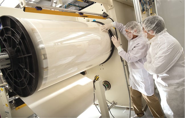
Figure 1. An example of flexible Willow Glass wound on a spool. The glass has been optimized for thin, lightweight, and conformally shaped applications and is also compatible with R2R device manufacturing. Glass width: 1.3 m; length: 300 m; thickness: 100 µm. Courtesy of Corning.
The specific flexible glass attributes that distinguish it from alternative polymer film or metal foil substrates arise from the composition and forming process. For example, it has thermal compatibility >500 °C, surface roughness (Ra) <0.5 nm, a water vapor transmission rate below the measurement detection sensitivity (<3 × 10⁻⁷ g/m2/day), and optical transmission in the visible spectrum limited by the air-glass interface reflection. At this thickness, the glass is flexible, which enables R2R high-throughput manufacturing processes, as well as applications that require a conformally shaped form factor.
Devices can be fabricated on the flexible glass using either sheet processing or R2R processing methods. For sheet processing, the flexible glass can be cut to size and handled as a free-standing part. Depending on the substrate size and handling system, though, temporarily bonding it to a process carrier may be needed. This allows for its use in equipment sets designed for rigid substrates. In this case, a debonding process occurs at the end to release the flexible glass device from the carrier. For R2R processing, the flexible glass web can be slit to appropriate widths, and leader and trailer materials can be applied for roller-system conveyance.
Device fabrication
By using either sheet or R2R approaches, a wide variety of device fabrication processes have been performed on flexible glass substrates. These include: vacuum deposition, photolithographic and laser patterning, printing, solution coating, and lamination. In addition, laser writing of embedded optical wave-guide interconnects and formation of through-glass vias have also been performed on flexible glass substrates. With these demonstrated process capabilities, electronic and optoelectronic devices that are routinely fabricated on thicker rigid glass substrates can also be manufactured on flexible glass. The key difference is that flexible glass opens up new, thin, lightweight, and conformal form factor applications, or applications dependent on high-throughput scaling of R2R processing not accessible to rigid substrates.
Glass has already established itself as the substrate of choice in mobile devices. The material plays a key role in the design and performance of current electronic and optoelectronic devices.
Based on the flexible glass attributes and processing capability, a wide variety of electronic and optoelectronic devices have been demonstrated on flexible glass substrates. Representative device examples include flexible glass sensors, displays, photovoltaics, antennas, and lighting. The flexible glass touch sensors were projected capacitive multipoint touch sensors based on both patterned ITO (indium tin oxide) as well as printed metal mesh designs. Printing and Cu (copper) plating metal mesh structures with linewidths <10 µm have been demonstrated in both sheet and R2R processes. Displays fabricated on flexible glass, such as active matrix liquid crystal, cholesteric liquid crystal, and electrophoretic displays, have highlighted the achievable thin and curved form factors that are possible. Flexible glass photovoltaic devices, such as CdTe (cadmium telluride), organic, and perovskite technologies, have highlighted the lightweight designs and path to high-throughput R2R processes to address scaling and manufacturing costs. Antennas have focused on transparent designs for integration within windows or objects with optical surfaces and target the growing number of communication channels.
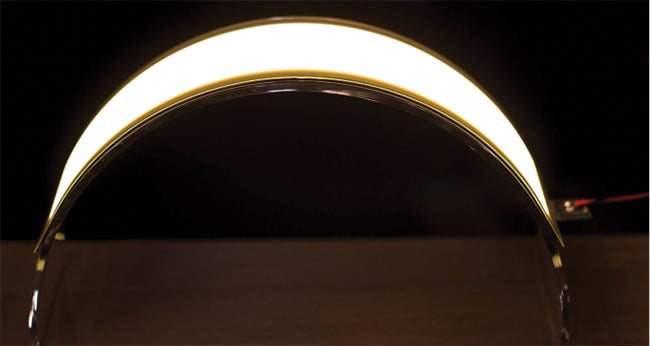
Figure 2. OLED lighting with flexible glass substrates provides thin, curved, space-saving designs with associated low weight. Courtesy of OLEDWorks.
OLED lighting fabricated on flexible glass (Figure 2) has also highlighted the thin, space-saving design, associated low weight, and curved form factor that is achievable. These representative applications utilize the advantageous properties of flexible glass, such as hermeticity, optical and surface quality, dimensional stability, thermal capability, and process compatibility. A key theme is the ability to scale using high-throughput R2R manufacturing processes.
Applications
At this point, it’s interesting to consider potential applications that can fully utilize the ability to fabricate high-quality electronic and optoelectronic devices on glass substrates hundreds of square meters in size. An example is the interactive wall or smart surface mentioned earlier that has integrated functionality to enable increased connectivity and interaction with the environment. This application combines the ability to fabricate devices on flexible glass substrates with the ability to perform large-scale lamination to other surfaces.
These laminated stacks can include high-resolution decorative patterns or images to create an aesthetic surface (Figure 3). With the flexible glass as the outer layer, it also creates a surface that is durable and compatible with typical cleaning products, which is important for health care and educational settings. Large-area smart surfaces can be created by integrating electronic functionality — such as sensors, displays, photovoltaics, antennas, or lighting — onto the flexible glass within this laminated stack. This creates a new level of interactivity and is enabled by the unique aspects of flexible glass for device fabrication, as well as compatibility with large-scale processes and integration.
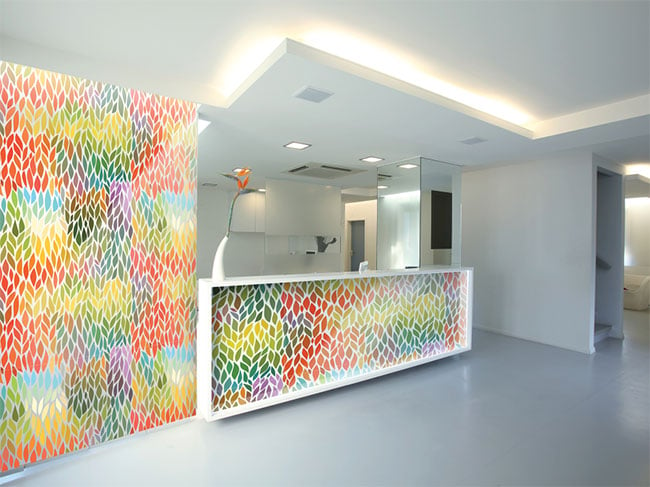
Figure 3. Flexible glass laminate enables large-area smart surfaces to integrate electronic functionality — such as sensors, displays, photovoltaics, antennas, or lighting — into this laminated stack. Courtesy of Corning.
Pursuing applications such as smart walls and interactive surfaces requires developing new ecosystem capability. It is necessary but not sufficient that flexible glass exists at a large scale. Complementary capabilities must also exist for processing the flexible glass to fabricate and integrate devices at manufacturing scales. Although these process capabilities and equipment designs are known, the ecosystem needs to be further developed to establish the pilot-scale and manufacturing capability.
Disruption ecosystem
One indication that a disruptive flexible glass ecosystem is emerging is that scaled equipment sets specifically optimized for R2R processing of flexible glass web are being designed and established. Representative scaled processes include vacuum deposition, printing, solution coating, and microreplication (Figure 4). A recent R2R vacuum deposition system (VON ARDENNE, FOSA LabX 330 Glass) designed for glass web processing is an example. Highlighting the scale in this emerging ecosystem, multiple R2R device processes have been demonstrated with flexible glass web with widths ≥1 m and lengths ≥100 m running at conveyance line speeds of ≥30 m/min.
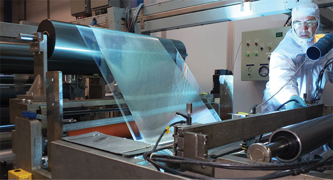
Figure 4. Large-scale optical diffuser coatings patterned by R2R microreplication on flexible glass web. Courtesy of Corning.
Flexible glass offers advantages for new applications, device designs, and fabrication processes not possible or practical with alternative substrate materials. Its distinguishing attributes include optical and surface quality, dimensional and thermal stability, and hermeticity. Flexible glass enables electronic and optoelectronic devices that have thin, lightweight, and bent or curved form factors. These functional devices can also be integrated into scaled applications. A disruptive ecosystem is emerging to specifically process and integrate flexible glass devices at a manufacturing scale. In these emerging applications and in the overall ecosystem, the flexible glass substrate is poised to be a central element that strongly influences device design, manufacturing, and performance.
Meet the author
Sean Garner received a B.Eng. in engineering physics from Stevens Institute of Technology in 1993 and a Ph.D. in electrical engineering from the University of Southern California in 1998. Since then, Sean has been working at Corning’s Science and Technology center; email: [email protected].
References
1. S.M. Garner (Ed.) (2017). Flexible Glass: Enabling Thin, Lightweight, and Flexible Electronics. Hoboken, N.J.: Wiley-
Scrivener.
2. S. Garner et al. (Oct 15-18, 2017). Flexible glass applications and process scaling. Lecture presented at AIMCAL in Tampa, Fla.