From minispectrometers to lithography, applications for MOEMS are expanding.
Following the path of semiconductors and mechanical devices, optical systems are shrinking in size and growing in capabilities, thanks to micro-optoelectromechanical systems (MOEMS). These combine electronics with mechanical and optical components. Examples include digital light-projection devices and minispectrometers, with applications such as projection systems, 3D printers, and instrumentation.
MOEMS promise better systems and solutions, but there is a need for further improvement and innovation to address integration and cost.
Eric Mounier, senior technology and market analyst for MEMS and Sensors at Yole Développement, predicts a bright future for the technology.
“The MOEMS market was $865 million in 2016, with more than eight million units shipped,” Mounier said. “In 2022, Yole Développement forecasts market value will be $1249 million with almost 30 million units shipped. It is almost five percent CAGR [compound annual growth rate] in value.”
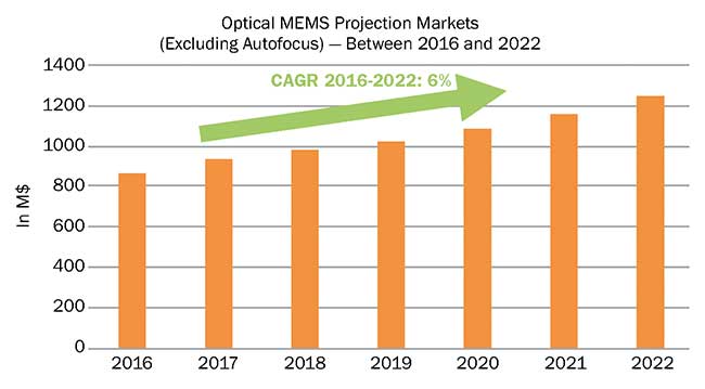
The market for micro-optical systems is projected to grow substantially. Courtesy of Yole Développement.
Most of today’s market is in projection, with micromirror MOEMS devices the bulk of current and forecasted future shipments. Today, micromirror devices hold a commanding position in such applications as cinema. Future growth prospects for this and other types of MOEMS lie elsewhere, including automotive applications, and also with ultrashort throw laser TV (or mobile TV), where a small, portable projector is used to create a large viewing screen on a nearby surface.
Wafer-level packaging
A big challenge for MOEMS is lowering the cost of packaging and integration, Mounier said, as is the case with other optical systems.
“However, both volume increase and innovative technologies, like WLP, or wafer-level packaging, will drive the cost down for a wider market diffusion,” he said.
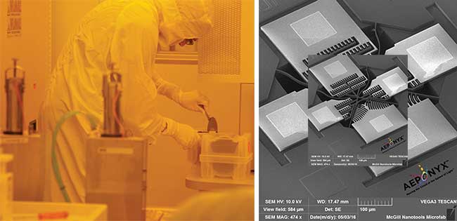
MOEMS devices, such as the one shown here, are fabricated in a cleanroom. Courtesy of Aeponyx.
Dallas-based Texas Instruments (TI) is a leader in MOEMS, with its micromirror-based devices accounting for the bulk of MOEMS devices shipped. Mike Mignardi, technology development manager for DLP (digital light processing) products at TI, said the company’s devices come in one of four nodes that range in pixel size from 13.8 µm down to 5.4 µm. The smaller the pixel size, the smaller the form factor for a given pixel count, and the faster the device micromirrors can be switched from on to off, or vice versa. The micromirrors themselves are aluminum-based, which means they offer optical capabilities across a broad spectrum.
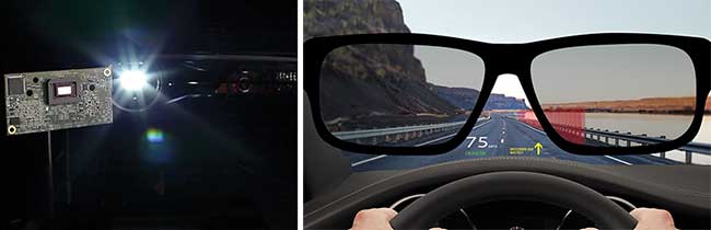
Micromirror-based optical systems are beginning to be used in automotive applications, such as smart adaptive lighting (left), that change lighting based on the situation and for head-up displays (right). Courtesy of Texas Instruments.
“As an optical MEMS device, we certainly push and steer photons,” Mignardi said. “We’re … looking at spaces other than visible. … [and] playing in the UV space and the IR space.”
For instance, the wide spectral output of TI MOEMS devices is being used in lithography to make printed circuit boards. The desired pattern of connecting traces on a board are loaded into a lithography system and translated into an array of mirrors, on or off. This is then projected onto the photopolymer on the board and eventually through processing, into the final metallic traces.
A key advantage of this approach is that it eliminates the need for masks. Thus, changes to the circuit board layout can be done on the fly, and smaller or more customized board runs become more economical.
UV, visible, and IR are also being used in high-volume 3D printing. The ability to get the right wavelength needed to photoactivate or sinter a material is important for this application.
The spectral range possible with a given device is a function primarily of the window that sits above the mirror and lets the photons in, Mignardi said. By changing the antireflective and other coatings on the window, TI sets the spectral response of the device to different bands in the UV, visible, and IR. The lower end is about 360 nm; the upper end is roughly 2500 nm.
The cost of the finished product breaks down to the device, package, and testing, Mignardi said. For packaging, TI is using a wafer-level approach — an entire wafer, which may contain many hundreds of devices, is packaged in one operation.
TI is just starting to get into the automotive market, where MOEMS devices can be used for a head-up display so that drivers can get information and directions without having to take their eyes off the road. The technology can also be used for smart adaptive headlights, where the beam is directed as needed. This may mean that it is aimed away from oncoming cars, allowing bright headlights to be used without fear of blinding other drivers.
The technology has other uses, too.
“I can display something on the road to tell the driver to turn here. Or I can highlight a pedestrian on a sidewalk to let the driver know that somebody’s over there,” Mignardi said. “Pay attention to that person.”
Finally, small MOEMS devices could resolve a big problem confronting consumers, Mignardi said. As TVs swell to 70 in. and larger in diagonal screen size, simply moving and mounting a TV in a small home or apartment becomes difficult and potentially dangerous. A 12- × 6- × 6-in. footprint micromirror MOEMS-based portable TV system can project a 70- or 100-in. picture on the wall, making it possible to avoid the problem presented by large flat panels without sacrificing visual quality.
“The TV looks just as good as a flat-panel display or even better,” Mignardi said. “It’s a laser display so the colors are really good.”
Virtual user interface
Bosch Sensortec of Reutlingen, Germany, has its own MOEMS mirror technology, with possible applications in virtual user interfaces and augmented reality, according to Lucas Ginzinger, head of the Optical MEMS product area. The company’s technology, he said, makes it possible “to project a user interface to almost every surface you can imagine, even if curved or graded. Our interactivity solution enables a wide range of possible input, from classic touch to gesture control.”

Micro-optical devices can project an interactive user interface, as shown here with this coffee maker. Courtesy of Bosch Sensortec.
Potential applications include smart speakers, home applications, and others. An application was launched at the 2018 Consumer Electronics Show with the debut of a smartwatch from China-based startup Beijing ASU Tech that could project a virtual screen on the back of a user’s hand.
The augmented reality uses involve projecting data onto surfaces, objects, or even into the eye. This allows data to be overlaid on top of a scene, thereby presenting the user with information about nearby objects of interest.
MOEMS technology could be used to do more than simply generate images and pictures. Three-dimensional sensing, for instance, could be an application that would benefit from the ability to steer light in precise patterns to enable structured illumination.
MOEMS technology could be used to do more than simply generate images and pictures. Three-dimensional sensing, for instance, could be an application that would benefit from the ability to steer light in precise patterns to enable structured illumination. Measuring the distortion of a known light pattern, such as beams that intersect to form squares, can yield 3D information about a surface or object. Machine vision is also a possible application.
Ginzinger predicted strong growth for MOEMS devices and applications, but he also noted there are challenges that will require R&D and product innovation.
“Especially for future-oriented applications,” he said, “we believe that size and cost of the light source will be one of the bigger challenges.”
Alternative to mirrors
Some MOEMS approaches use optical components other than mirrors. For example, startup Aeponyx of Montreal uses electrostatically actuated MEMS and silicon nitride waveguides. In response to changing voltages, these waveguides bend and move, redirecting light. Aeponyx is bringing a product based on this approach to market in 2019 with a micro-optical switch intended for use in telecom access networks and data center applications.
“For the switch itself, our key advantage is our switching speed compared to 3D MEMS,” said Philippe Babin, CEO of Aeponyx. He added that their approach also offers a tenfold reduction in cost and a smaller size for their solution.
The technique requires the use of stress compensation and management in the MOEMS structures, which consist of silicon nitride in a silicon dioxide sandwich sitting atop a silicon-on-insulator wafer. The arrangement leads to stress in the films — this must be accounted for.
Another nonmirror MOEMS approach comes from Silicon Light Machines (SLM) of Sunnyvale, Calif. SLM’s products are built on a high-performance spatial light modulator composed of thousands of free-standing silicon nitride microribbons anchored on the surface of a silicon chip. The deflection of the ribbons is electrostatically controlled, making the product a programmable diffraction grating or what the company calls a grating light valve. Light, typically a laser beam, can be attenuated, modulated, and switched as desired.
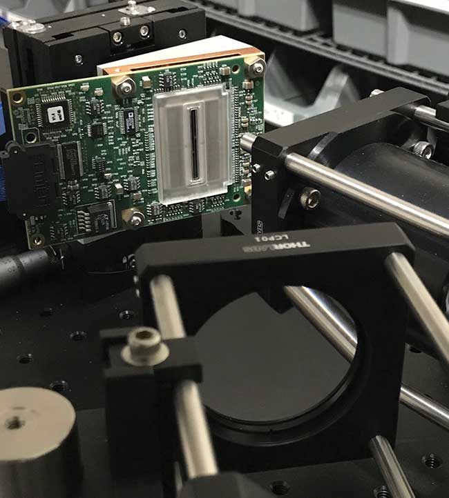
A grating light valve, which is a spatial light modulator, in an optical engine. The device can modulate, attenuate, and switch light. Courtesy of Silicon Light Machines.
SLM’s devices are used in printing and lithography machines by its parent, SCREEN Holdings Co. Ltd., of Japan.
“Each little element will diffract or reflect light,” said SLM’s CEO Lars Eng. “You can very, very precisely give a dose [of light] to your media.”
The technology can also be used in machine vision to create a structured illumination source or to steer a lidar beam. It could be used for materials processing, for example, to mark parts with an identifying pattern or designation.
SLM’s programmable gratings today have a linear array of 8192 channels, with work underway to go to higher counts and 2D arrays. Research and development is also underway — one goal is a power capability of up to 10 kW.
Beyond that, the task is figuring out how to solve a customer’s problem using the technology. “The big challenge,” Babin said, “is finding the right fit with the application.”