Leveraging innovative fabrication technologies, freeform micro-optics are redefining the landscape for general lighting, anti-counterfeiting, and other applications.
CHRIS RICH, JOHN TAMKIN, AND KENT COULTER, WAVEFRONT TECHNOLOGY INC.
Much attention is given to freeform optics fabrication, which has improved the performance of traditional micro-optic imaging systems1. But replicated freeform micro-optics are also fostering advancements across a broad spectrum of applications beyond the realm of traditional imaging. These applications range from virtual reality (VR) displays, commercial and consumer lighting2, solar panels3, anti-counterfeit devices, and product branding.
Existing design software — such as
LightTools, CODE V, Zemax, and Trace-
Pro — is adequate for the development of conventional freeform optics. For replicated micro-optics, however, feature sizes range in scale from the submicron to hundreds of microns in size.
The optical design community is also faced with the challenge of developing
tool sets that integrate previously disparate models. For example, modeling waveguide transport requires solving Maxwell’s equations. Yet traditional optical design software uses ray tracing for simulation. The demands of these two worlds need to converge when developing optics systems that employ a hybrid approach, such as holographic VR displays4. The same applies to research combining the world of freeform micro-optics with holography to produce freeform holograms5.
As a result, tools are needed that can bridge the gap between conventional and emerging micro-optic concepts to improve the design workflow. Companies such as Synopsys are starting to integrate
CAD platforms such as RSoft that have traditionally been used to design photonic structures and waveguides with LightTools illumination design software, which became a workhorse in the lighting design community by seamlessly creating and transferring bidirectional scattering distribution function information.
The challenges continue even after a design meets all optical requirements, as it must then be translated into a production sequence. For example, WaveFront recently completed a design that required over 10,000 microfacets, where each microfacet maintained a unique angle. Translating the design into production required specialized processes and software, along with multiple diamond geometry changeouts, to achieve financially acceptable tooling origination times.
Next-generation roll-to-roll (R2R) manufacturing technology presents a potential solution for expanding the design space for both imaging and nonimaging optics and navigating them through production (Figure 1).
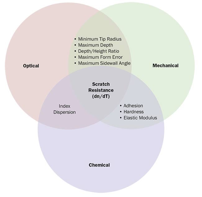
Figure 1. Design rules for roll-to-roll (R2R) replication of optics. dn/dT: temperature coefficient of the refractive index. Courtesy of WaveFront Technology.
Freeform micro-optics can be fabricated at low cost using Cast and Cure R2R embossing methods6. Their production design can take advantage of existing simulation and optimization software. Micro-Fresnel lenses must have minimum draft angle to ensure good release during embossing. Facet width and depth are limited by diamond tool fabrication geometries. Tip radii of microprismatic surfaces contribute to scattering. Small tip radii are better, but sharp tips can break off during production. Software such as LightTools can both adjust the tolerance of and optimize these production-specific characteristics.
R2R technology has traditionally been limited to manufacturing single-sided optical surfaces such as diffusers, simple prismatic structures, or gratings and lenticular arrays. The technology was also critical to the expansion of flat-panel display technology and is now finding its way into LED lighting. Next-generation R2R embossing will further allow accurate registration of front to back with positioning errors of less than 5 µm over large areas (greater than 500 mm) at production speeds.
Origination methods
When replicating optics comprising single elements or relatively small arrays, the original element can be fabricated using diamond turning or semiconductor lithography processes, including grayscale lithography. More recent innovations such as 3D microprinting of optical-grade surfaces using two-photon lithography or additive manufacturing have also proven to be viable for short runs and fast turnaround.
R2R fabrication technology, however, offers the lowest price per square inch for products that must meet aggressive price points.
Replicating micro-optic structures requires a mold or master tool, which is transferred to a drum using a nickel shim or other technology. To make the master tool, an original pattern is replicated from a parent part to a child part using a step-and-repeat process. This tree of replication can have multiple generations before the final structure is transferred to a drum.
The exception to this process is when the pattern is directly cut into a copper or nickel embossing drum using a horizontal drum lathe. Diamond-turned complex microprismatic structures also have the smallest tip radii, leading to very small amounts of scatter from the structure. Horizontal drum lathes have typically been used to make LCD diffuser films and are typically single-purpose machines. However, these precision tools can be outfitted with additional equipment such as fast tool servo accessories, rotating B-axis stages, and live tooling to generate complex freeform patterns directly into the embossing drum (Figure 2). Both imaging and nonimaging optics can be cut in the same drum with positioning accuracies at the micron scale.
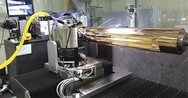
Figure 2. A five-axis horizontal drum lathe. Courtesy of WaveFront Technology.
Replication
While design, modeling, and tooling define the original microstructure, the ability to accurately replicate microstructures onto a film surface using heat, pressure, and/or Cast and Cure R2R processes requires precision control of positioning, tension, temperature, and curing.
For nanometer resolution, UV-cure R2R processes offer a unique high-quality embossing method that produces a wide variety of web products, including custom-engineered structures, lens structures, specialty optical film, prismatic films, and multicomponent devices. The microstructured films are typically manufactured with widths ranging from 6 to >60 in. in cleanrooms via custom-built R2R equipment (Figure 3). Replicated features can range from a few nanometers to >150 µm in height.
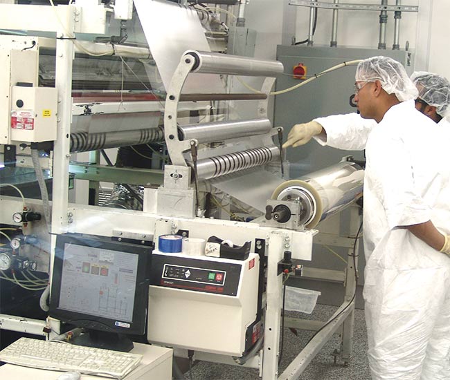
Figure 3. A custom-built UV embossing R2R replication system. Courtesy of WaveFront Technology.
The substrate is a critical component of the optical structure design, with UV casting applicable to substrate thicknesses of 12.5 to 300 µm. The substrate can be a variety of materials, as long as it has an appropriate index of refraction and a thermal expansion coefficient that meets the design requirements. The replication process allows designers to choose substrates that are compatible with other materials and processes in the optical system.
The UV-cure R2R technique supports replication of surface-relief microstructures that must meet stringent tolerances, including diffusers, optical elements, lenses, gratings, or lenticular structures.
It routinely embosses surface textures with depths of between 10 nm and
200 µm. Rolls of material can be made clear for transmissive products, or coated with metal or dielectrics to customize the optical response. Recent advancements have demonstrated the ability to emboss microstructures into resin films that can then be peeled from the substrate to produce standalone devices on the order of 3 to 5 µm in thickness.
The introduction of high-precision, double-sided components opens several
new applications. By replicating structures on both sides of a substrate, a beamsplitter grating on the front surface can
be combined with focusing microlenses on the back surface. UV embossing further allows fabrication of double-sided refractive and diffractive optical elements
through a wafer-scale replication process that combines the alignment and positioning accuracy of photolithographic processes with the low fabrication costs of an R2R replication process. The combination of high precision and low cost makes these components ideal for a range of previously unexplored market opportunities.
Lighting applications
Micro-optical components for LED lighting are designed to shape the light, optimize homogenization, and enable large-area visual elements such as texture, patterns, and depth. These large-area elements are composed of microstructured optics that contain films and sheets to guide, reflect, and refract light.
With the increasing popularity of LED lighting, the need for engineered photometric control has grown. Yet, a given supplier’s LED may not produce the precise emission profile. This problem can be remedied through the use of auxiliary optics, which include refractive (continuous-surface and microstructured), reflective (continuous and faceted), and diffractive optics. These solutions not only provide more photometric control over LED output but they can also impart aesthetic effects such as the appearance of depth and structure in a planar panel (Figure 4).
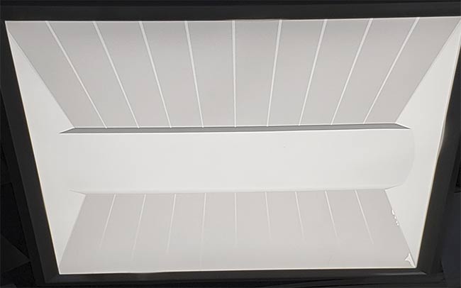
Figure 4. Recently launched 3D geometric patterns for 2D LED panels. Courtesy of WaveFront Technology.
There are several other lighting applications in which microstructures can potentially provide greater efficiency, aid installation, or offer aesthetic advantages where fine photometric control is required. Replicated micro-optics can also simply provide a more preferable distribution of illumination in applications such as signage, artistic lighting, markers for roads and runways, machine vision, automotive instrument panels, dome lights, and exterior brake and signal lights.
Anti-counterfeiting
Microstructured optical products can exhibit a 3D appearance and optically variable characteristics that provide an eye-catching difficult-to-replicate visual effect7. When applied to a document
substrate, such structures can serve as
effective anti-counterfeiting measures.
The simplest type of microstructured optical product can easily correspond each surface facet to a fixed shade of gray. The palette element consists of a uniform distribution of microstructured surfaces, with the sizes and angles varying between the surfaces to give different levels of reflectance.
In the case of portrait effects, the brightness of each microstructure pixel modulates as a function of its position within the portrait and in accordance with the grayscale value of each corresponding pixel from the input artwork.
There are two possible mechanisms for achieving this variable-intensity pixel behavior. The first is to fix the average slope of the microstructure pixels corresponding to the portrait image while also varying the curvature of the microstructure pixel surfaces so that the light is reflected into an expanding cone of light. Only part of the light will be intercepted by the eye at any one angle of view. The variable degrees of surface curvature represent the various shades of gray within a portrait image. This type of intensity modulation is difficult to achieve because of the inherent difficulty in the microsculpturing of such small surface areas.
A second, alternative technique is to modulate the reflected light intensity by varying the area of the microstructure surface. To create optically variable rows of light and dark, pixels are interlaced into corresponding rows of microstructured mirrors of different slopes. Then when the surface-relief microstructure is tilted about an axis that runs parallel to the rows of interlaced microstructures, the symbols will alternatively reflect light to the eye, depending on which set of microstructure surfaces is aligned for maximum reflection.
The microstructure optical product can generate various other optical effects as well. It can be embossed as a transparent optic, in which case the microstructure becomes a microprism array and the image becomes an optically variable watermark in transmission. Thus, as an observer looks through the transparent
substrate at a light source, an image switch appears to occur as the transparent device moves from a point above the light source to one below it.
Conclusion
The specialized area of freeform microstructure optics is quickly evolving, and the design, modeling manufacturing, and
application of unique structures is growing rapidly. Origination tools such as five-axis horizontal drum lathes with fast tool servos are now available to achieve these complex structures, and double-sided R2R UV-cured embossing is further providing cost-effective mass production techniques.
A range of new optical components is now within reach that can improve quality of life through a diversity of products, from LED illumination that delivers light more efficiently, to anti-counterfeiting measures that secure authenticity of products. As the market continues to demand higher performance in a smaller footprint, R2R delivery of complex freeform optics will continue to expand.
Meet the authors
Chris Rich co-founded WaveFront Technolgy Inc. in 1986 with Joel Petersen. Rich has over 30 years of experience and expertise in microstructure design, origination, and replication of precision optics on roll-to-roll platforms; email: [email protected].
John Tamkin, Ph.D., is vice president of R&D at WaveFront Technology. He has over 35 years of experience in optical systems engineering and lens design, as well as market experience ranging from medium-volume commercial products to lithography capital equipment. He has a doctorate in optical sciences from the University of Arizona; email: [email protected].
Kent Coulter, Ph.D., joined WaveFront Technology in July 2020, bringing 15 years of experience as a program director at Southwest Research Institute, as well as 10 years as director of science and technology at JDS Uniphase (now VIAVI). He has a doctorate in physical chemistry from Texas A&M University; email: [email protected].
References
1. J. Bec et al. (2019). Broadband, freeform focusing micro-optics for a side-viewing imaging catheter. Opt Lett, Vol. 44,
pp. 4961-4964.
2. C. Leiner et al. (2019). The potential of freeform micro-optical elements on light management foils. In Optical Design and Fabrication 2019 (Freeform, OFT), OSA Technical Digest (Optical Society of America), Paper No. FW4B.5.
3. X. Zhang et al. (December 2014). Roll-to-roll embossing of optical linear Fresnel lens polymer film for solar concentration.
Opt Express, Vol. 22, Issue S7, pp. 1835-1842, www.doi.org/10.1364/oe.22.0A1835.
4. Y. Zhang et al. (2019). Modeling and optimizing the chromatic holographic
waveguide display system. Appl Opt,
Vol. 58, pp. G84-G90.
5. S. Schmidt et al. (2020). Tailored micro-optical freeform holograms for integrated complex beam shaping, Optica, Vol. 7,
pp. 1279-1286.
6. U. Palfinger et al. (March 14, 2018). R2R fabrication of freeform micro-optics. Proc SPIE, Vol. 10520, Laser-based Micro- and Nanoprocessing XII, Article No. 105200J, San Francisco.
7. WaveFront Technology Inc. (Oct. 23, 2015). Optical products, masters for fabricating optical products, and methods for manufacturing masters and optical products. U.S. Patent No. 10,859,851. Washington, D.C.: U.S. Patent and Trademark Office.