
Full-Immersion AR: The Path to Consumer-Friendly Devices
High-refractive-index glass waveguides may awaken an end-consumer-device industry ecosystem.
By Ruediger Sprengard
Augmented and mixed reality (AR/MR) devices are perceived by some as the next big thing in consumer electronics. These devices could form the basis of the next great computing revolution, joining the ranks of smartphones and personal computers as a foundational technology that changes the way we live, work, and play.
But getting an AR/MR consumer-grade product ready for mass-market adoption is still a challenge. The industry that makes AR/MR hardware has not yet delivered a lightweight device with the wide field of view (FOV) necessary to create a fully immersive environment.
AR/MR devices impose a digital reality on the real world. Anyone who has played games such as Pokémon Go or Harry Potter: Wizards Unite has used
AR. These games, while popular, require users to mediate their experiences through their smartphone, a less-than-ideal experience because the screen is small and because the user must continuously involve at least one hand with the smartphone.
Wearable AR/MR devices, such as smart glasses and other head-mounted display units, are not commonly seen in everyday settings. Tech companies have seeded devices to developers, and occasionally such devices appear in workplaces, where use cases include safety training or helping warehouse workers locate items. Ford Motor Co., for example, uses AR to enable vehicle designers to
see renderings of potential changes overlaid on top of a physical prototype. But high expense and low ease of use puts
AR devices out of reach for most consumers. Currently, annual sales figures number about 300,000 units, far fewer than the tens or hundreds of millions of units that consumer-grade AR devices could generate.
The past 12 months have seen remarkable advancements and a steady stream of new product announcements in this space. The vast amounts of money invested by corporations and venture capitalists, together with the increasing success of industrial use of AR/MR smart glasses, has provided a vital proof of concept and starting point for consumer-grade devices. Already, the smart glass industry has become the beneficiary of a burgeoning manufacturing ecosystem built broadly around a few key ideas that may form the basis of consumer-grade AR.
Basic components of smart glasses
Smart glasses are treading the familiar direction of many technologies, in which early adopters and commercial applications provide a crucial early market for prototypes. Across the industry, smart glasses share basic forms. AR optical hardware generally comprises three components: an image-generating unit, an optical projection system similar in functionality to the optical engine in a conventional projector, and the optical combiner, which projects the image into the human eye.
The ideal smart glasses are lightweight (significantly less than 100 g) and look like ordinary eyeglasses used to correct vision. This hardware form factor, however, imposes a series of constraints on the components. In current designs, the projection surface is relatively close to the pupil — just a few centimeters away — making it challenging to achieve a wide FOV and a large eye box without the use of high-index materials in combination with a waveguide approach. It is likewise difficult to enable a wide FOV when the projector is close to the projection surface1,2.
To overcome these constraints, designers of AR optical systems have begun turning to projection surfaces with material properties that enable a wider FOV.
Waveguide technology
Many optical architectures under development are on the path to consumer-grade AR, and some are quite advanced. Waveguide-based systems are considered the most promising optical approach to solving the conflict between wearability (small form factor, a large eye box, and minimum weight) on the one hand, and a fully immersive user experience (wide FOV and crisp, bright images) on the other, while retaining acceptable optical efficiency. Such waveguide-based systems may — depending on the specific light management technology used and the requirements of the end application — consist of only one layer of waveguide transmitting all three colors (RGB), a stack of separate waveguides for each color, or two waveguides conducting RG and GB, respectively. A stack of up to six waveguide layers is used to provide an
authentic 3D experience, with two or more focal planes of the virtual image.
So how does this waveguide work? From an end user’s perspective, a waveguide looks just like a regular piece of glass, the type that is used to make corrective lenses. In fact, with the waveguide as a flat piece of glass, it is even possible
to combine an optical system with corrective lenses, theoretically making smart glasses easily accessible for large populations.
The optical functionalities of such waveguide-based combiners can be divided into several fields (Figure 1). First, an incoupling structure redirects the image originating from the projector into the acceptance angle of the waveguide. The image of the projector illuminated onto the waveguide glass has a very small spot size. To enable a large FOV, along with high flexibility of the optical system to adapt to the individual interpupillary distance of the user, an eye box as large as possible is required3. Consequently, the image beam must be expanded. This beam expansion is the second functionality. Then, over the area of the eye box,
the image beam must be selectively extracted into the user’s pupil; and finally, from the incoupling point to the outcoupling point, the light ray travels over many centimeters. The light ray will be captured within the glass waveguide as long as the light is hitting the inner surface of the glass within the limits of the angle of total internal reflection (TIR), which is related to the refractive index of the glass. To help make the light-management structures (incoupling, beam expansion, and outcoupling) work as accurately as possible with the ideal optical design (generated by computer algorithms), the ideal waveguide glass will not modify the beam but will transport it along the predicted trajectory.
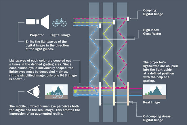
Figure 1. An illustration of the waveguide technology using various layers for RGB, with (in)coupling and outcoupling structures. Courtesy of SCHOTT AG.
Before discussing such mechanisms in detail, two approaches to realizing the light-management functionalities in waveguide-based devices are described.
Surface-relief gratings
Surface-relief gratings are based on the principles of diffractive optics and represent the most common approach in the AR/MR industry. Today, this technology already combines high image quality with a reasonably mature ecosystem of manufacturing equipment and materials. There are two manufacturing approaches: 1) nanoimprint lithography (NIL), where the grating structures are impressed into an organic resin with subsequent freezing via (photo)polymerization of the resin; and 2) reactive ion etching, where diffractive optical surface structures are generated through dry etching processes that combine physical and chemical processes — a technology applied in micro- and nanofabrication. Given the complexity of the optical modeling, diffractive waveguides have a high optical design barrier. Furthermore, they are intrinsically limited in optical efficiency.
Volume holographic gratings
Volume holographic gratings may provide an interesting alternative to surface-relief gratings. In this case, thin-film polymer (liquid-crystal-based or photopolymer) is exposed by laser light to embed microscopic nanoscale holograms, modifying the function as mirror-like optics. Again, incoupling and outcoupling structures are used. Currently, the image quality (haze and color uniformity) and manufacturing maturity of volume holographic gratings mean they are considered to be less advanced than surface-relief gratings.
Reflective waveguides
The use of reflective waveguides follows a different strategy. The light beam that travels along the glass waveguide passes a series of slanted, partially reflective mirrors realized by optical coatings embedded in the waveguide. Each mirror projects part of the visual information toward the human eye and partially transmits the rest of the light, which continues to propagate along the waveguide until it hits the next partially reflective mirror. Here, another portion of the light is extracted. The technology is widely acknowledged to achieve good image performance, such as high resolution. This enables, for example, very good readability of the image. Along its innovation road map, reflective waveguide technology must deliver on smaller projector systems positioned in the arm of the glasses, a large eye box, and a wider FOV. This technology has been successfully applied in several commercial smart glasses. Manufacturing is based on conventional optical manufacturing technologies but requires mastering of tight tolerances under cost-efficient, high-yield, mass production setups.
Wafer properties
The physiology of human vision is complicated. Visual capabilities are determined by the performance of our optical system (the human eye) and its image processing unit (our brain receiving the information as an electrical signal via nerves). To deliver the promise of a fully immersive experience, the virtual FOV should be identical to our natural FOV. Human binocular vision has an FOV of approximately 120°, with symbol recognition occurring within 60°. So far, the best FOV achieved by commercial AR devices on the market has been 43°.
What is limiting the FOV? Identical to its one-dimensional exploitation in optical fiber communication, the key property for any material used as a waveguide is its refractive index, or more precisely, the difference of the refractive index of the waveguiding glass and the surrounding medium (typically air in the case of AR glasses). A higher refractive index affects FOV (Figure 2).
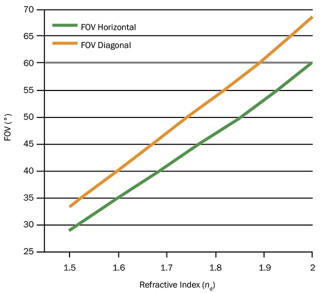
Figure 2. Correlation of refractive index and FOV for surface-grating-based waveguide systems. Courtesy of SCHOTT AG.
For years, the development of waveguides was limited by the progress of high-index materials. Some investigators pinned their hopes on polymers because polymers are low weight. However, the basic chemistry of optical polymers tends to rule out a high index. Also, polymers do not achieve the unparalleled optical
properties of glass when it comes to homogeneity, absence of stress birefringence, or surface roughness. Polymers tend to degrade over time, especially under high light intensity, which is likewise unacceptable in a consumer product. Similarly, glass wafers used for years in the semiconductor and optoelectronics industries seemed a likely candidate. These wafers, however, are limited to a “normal” refractive index (~n = 1.5), which is too low for AR applications. The wafers also do not meet geometrical wafer quality requirements. (More on this later.)
Currently, the most common refractive index of glass wafers used in the market is 1.8, with recent developments offering 1.9 to waveguide designers of next-generation devices. Driven by the need for an even wider FOV, a joint industry effort is underway to investigate the technical
and commercial feasibility of using 2.0 glass wafers in AR devices. Among the technical challenges to achieving a higher refractive index are the abilities to achieve a high(er) transmission for short wavelengths, to decrease the specific weight of the materials (because of the heavy atomic nature of the chemical species used to achieve higher refractive index), and to realize aspects of glass manufacturability (such as wide and thick preforms for 300-mm wafers) under mass production conditions.
What else makes a suitable waveguide? From a mass manufacturing reality: optical properties, geometrical properties, and commercial availability.
When it comes to optical properties — other than refractive index — the ideal waveguide material does not modify the image beam. This is because the AR system is sensitive to the effects of absorption (which leads to lower light efficiency in the optical system, resulting in the need for stronger light sources that consume more battery power), scattering of light (which causes a decrease of efficiency and a reduction in image contrast), stress birefringence (which results in undesired polarization-dependent effects), and local fluctuations of refractive index (which negatively affect the modulation transfer function, or MTF). MTF is a measure of the image-forming capability of the optical system.
With geometrical properties, the goal is to minimize their impact on beam quality. The ideal waveguide consists of two perfectly flat and parallel surfaces. Any local nonflatness of the surface directs the light reflected via TIR into a nonideal direction, causing distortion, loss of contrast, and loss of image brilliance. AR device manufacturers are driving glass wafer manufacturers to an unprecedented quality level. The key property is the so-called total thickness variation (TTV) — that is, the maximum difference between the thickest and the thinnest part of a wafer. In the past, manufacture of glass wafers used by the semiconductor or optoelectronic industries had the most demanding requirements: a TTV down to 5 µm, with a few applications requiring a special grade of 2 µm. This would be unacceptable for an AR waveguide system. When it comes to TTV, AR requires one order of magnitude better than these values. Only a few experienced waveguide suppliers have managed to achieve such a quality level under cost-efficient and highly consistent mass-production conditions4 (Figure 3).
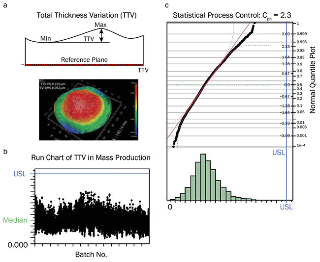
Figure 3. TTV is a key parameter that directly influences the image quality of a waveguide-based device (a). TTV values of SCHOTT’s process (b). The Cpk value of 2.3 underlines the excellent process capability (c). Cpk: process quality ratio. USL: upper specification limit. Courtesy of SCHOTT AG.
Smart glasses intended for everyday use, theoretically mediating all activities over a day, must be comfortable to wear and must look like ordinary eyeglasses. Low weight is a key requirement, and AR product developers are fighting for every gram. Glass wafers may offer value here, if the specific density of the glasses can be decreased (without affecting their high refractive index) or the thickness of the glasses can be reduced (without affecting their high mechanical stability).
Waveguide system manufacture follows pricing logic similar to semiconductor or display manufacture: The larger the substrate, the lower the cost per device. Standard wafer diameters are 150 and 200 mm. And 300-mm wafers are now available5 (Figure 4). In a combined effort, the industry is working to find the best commercially and technically viable balance in trade-offs between wafer size (manufacturing efficiency), wafer thickness (weight and handling robustness), geometrical surface quality (TTV), and material properties, including transmission and refractive index.
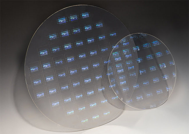
Figure 4. High-refractive-index glass wafers with 200- and 300-mm diameters and nanoimprinted surface gratings. Courtesy of SCHOTT AG.
In terms of market penetration, the AR market is still in its infancy. The global market is a few hundred thousand devices per year. Yet, devices for consumer use are expected to be launched in the foreseeable future. Because the requirements for AR waveguide wafers are unique, a supply chain with proven capabilities and capacities still needs to be built up. The existence of a reliable supply chain for glass wafers from willing companies that are capable
of quick ramp-ups in a cost-efficient setup is key. Currently, only a few suppliers have demonstrated a proven track record of
successfully serving the AR industry.
Ideas at the ready
Waveguide technology is considered promising for providing a fully immersive experience. Glass will remain the material of choice, given its unsurpassed quality at a more than competitive cost. A well-stocked innovation pipeline is ready to be implemented jointly with other industry players, and the business ecosystem is percolating as well.
Expect the pace of change to increase even more. AR has generated enormous research interest. While many challenges remain in the development of optical architectures, the road map for solving these challenges is largely apparent. This is giving value-chain players the confidence to invest, which will ultimately make smart glasses more affordable.
Meet the author
Ruediger Sprengard, Ph.D., is head of augmented reality, advanced optics for SCHOTT AG. Throughout his career, he has worked on advanced materials and components for optoelectronics and display applications. Sprengard has an educational background in solid-state physics. He is an SPIE member and author or co-author of more than 25 scientific papers and book contributions, and he holds 20 patents. Sprengard headed SCHOTT’s R&D and production ramp-up of a high-index wafer portfolio marketed under the SCHOTT RealView brand; email: ruediger.sprengard@schott.com.
References
1. B.C. Kress and W.J. Cummings (2017). Towards the ultimate mixed reality experience: HoloLens display architecture choices. SID Digest, invited paper, Vol. 32, Issue 1, pp. 127-131.
2. B.C. Kress (July 2019). Optical waveguide combiners for AR headsets: features and limitations. Proc SPIE, Vol. 11062, Digital Optical Technologies 2019, 110620J.
3. D.J. Grey (June 2017). The ideal imaging AR waveguide. Proc SPIE, Vol. 10335, 103350C-1.
4. R. Sprengard et al. (June 2019). High refractive index glass wafers for augmented reality devices using waveguide technology: recent advances in control of quality parameters and their correlation with device properties. SID Digest of Technical Papers, Vol. 50, Issue 1, pp. 116-120.
5. SCHOTT AG (August 2019). 300-mm SCHOTT RealView high-index glass wafers with nanoimprints: SCHOTT and EV Group pave the way for consumer-grade AR/MR glasses, press release, www.schott.com/english/news/press.html?NID=com5643.
/Buyers-Guide/SCHOTT-AG/c13194