Phase masks and phase plates made of fused silica are used for a number of applications in the field of optics and photonics. Examples include diffractive masks used in laser micromachining or structured illumination, and for the generation of specific focus geometries in high-resolution microscopy. Fused silica offers high transparency from the deep UV to the near-IR and excellent thermal and chemical properties. Phase masks fabricated from this material often require binary surface profiles with step heights that are comparable in magnitude to the wavelength applied, as well as lateral structure dimensions measuring from the millimeter to the micrometer scale.
In addition to lithographic techniques, direct laser structuring of fused silica is a suitable method for the fabrication of phase masks. However, due to fused silica’s high transparency, the latter approach places high demands on the laser process. Adequate absorption for the material is only available in the mid-IR or vacuum UV (VUV). Processing it with a CO2 laser at the 10.6-µm wavelength does not offer sufficient resolution for microstructured surfaces. In the VUV, the 157-nm wavelength of a molecular fluorine (F2) laser can be used, although economical production is hardly possible because these lasers deliver low power compared to what would normally be required. Fused silica can also be ablated using ultrashort-pulse lasers to induce multiphoton absorption. But, so far, optical quality surfaces cannot be produced in this way.
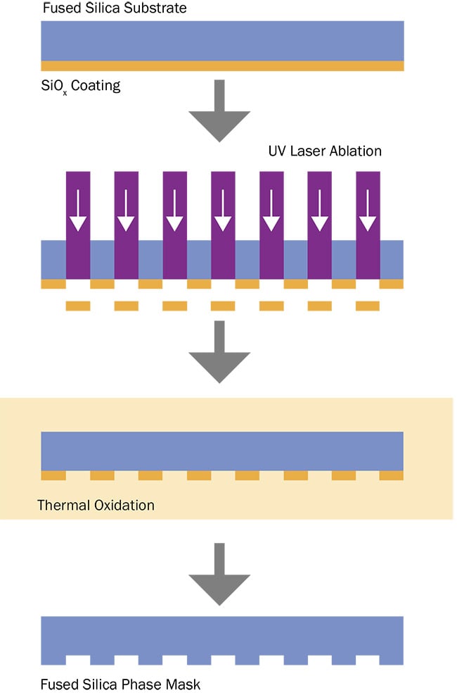
Figure 1. Laser structuring and thermal oxidation of SiOx for fabricating fused silica phase masks. Courtesy of IFNANO.
An alternative approach to fabricating phase masks begins by coating a fused silica substrate with silicon suboxide (SiOx), adjusting the thickness of the
layer to produce the required phase delay. To obtain the desired phase profile, the layer absorbing in the UV is structured
by laser ablation and converted into UV-
transparent SiO2 in a subsequent annealing process. This method produces a highly transparent and radiation-resistant phase mask made of pure SiO2, with
diffraction efficiencies close to the theoretical maximum, as well as good suppression of the transmitted zero order.
Silicon suboxide
SiOx (with x < 2) is a substoichiometric silicon oxide whose atomic structure depends strongly on its manufacturing method. The SiOx coatings described here are produced by thermal evaporation of silicon monoxide (SiO), which usually results in x approximately equal to 1. Other compositions can be obtained via reactive coating processes. SiOx layers are very stable at room temperature. At high temperatures (for example, 900 °C), SiOx oxidizes to SiO21. The incorporation of oxygen increases the layer thickness by approximately 30%. The oxygen deficit
of SiOx leads to considerable UV absorption (>105 cm−1 for wavelengths below 350 nm). This strong absorption enables the use of UV laser ablation to precisely structure SiOx films. This particularly applies in so-called back-side ablation methods, where the laser beam is directed through the transparent fused silica substrate onto the SiOx film. The “predetermined breaking point” between the substrate and the absorbing layer causes almost residue-free delamination and thus ensures optical surface quality.
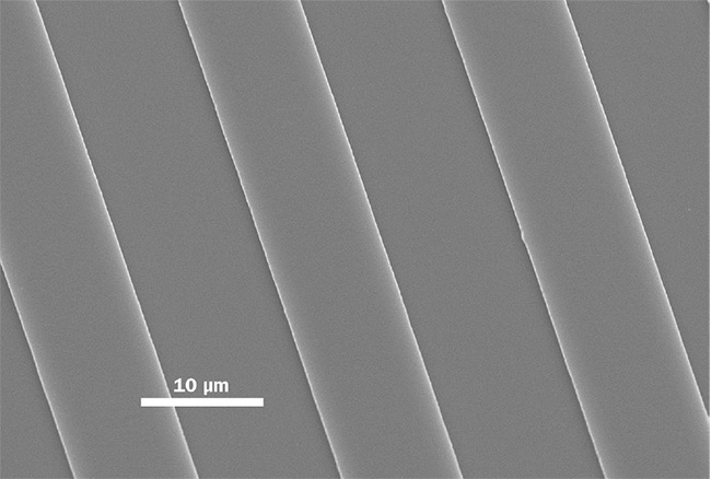
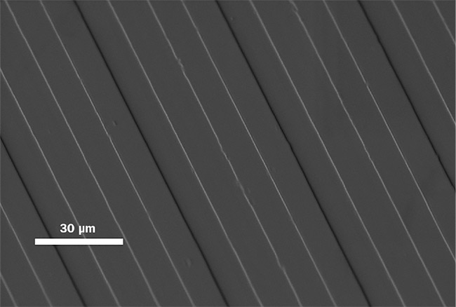
Figure 2. Scanning electron micrographs of a two-step fused silica phase mask (top) and a four-step fused silica phase mask (bottom). Courtesy of IFNANO.
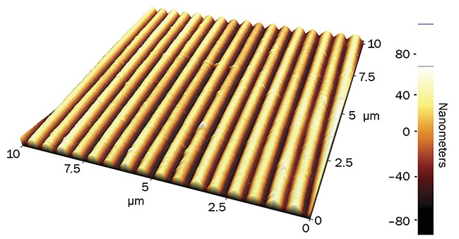
Figure 3. A 600-nm-period surface grating on glass made by single-pulse argon fluoride (ArF) excimer irradiation via phase mask projection. The surface profile has been recorded using an atomic force microscope. Courtesy of IFNANO.
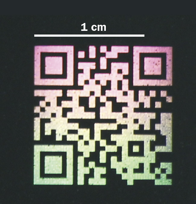
Figure 4. An iridescent quick-response (QR) code made by laser ablation on glass via phase mask projection. Courtesy of IFNANO.
Two-step phase masks
To produce a binary phase mask, the phase shift required for the desired operating wavelength — that is, λ — is first determined. For a simple transmission phase grating in which the zeroth diffraction order is to be suppressed, the required phase shift is λ/2. This can be realized by a relief grating with a step height defined as d = λ/(2 (n − 1))
(n = the refractive index of SiO2 at λ).
To achieve this step height, a SiOx layer with a thickness of λ/[1.3 × 2 (n − 1)] is deposited, which will grow to a thickness of d during the oxidation. Then the desired binary relief is created by (back-side) laser ablation (Figure 1)2.
The duty cycle (that is, the line width to spatial period) is 0.5. Excimer lasers are particularly suitable for this ablation process. They can be used to process a specified area at once via mask projection. Ablation with an argon fluoride (ArF) excimer laser requires a fluence of ~0.5 J/cm2.
For example, a grating line measuring several centimeters in length can be produced with a single-laser pulse by means of a slit projection. This leads to grating lines with extremely sharp edges versus lines inscribed with a Gaussian-shaped laser spot, where stitching phenomena can lead to poor edge quality. Since the substrate is completely exposed in the trenches, very good surface quality is achieved both on the stripes and in the trenches.
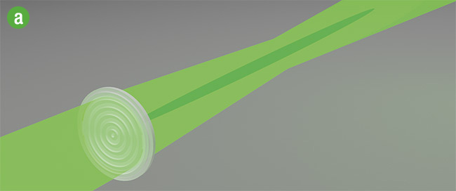
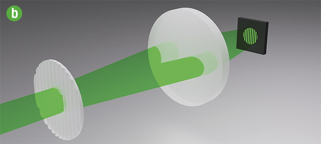
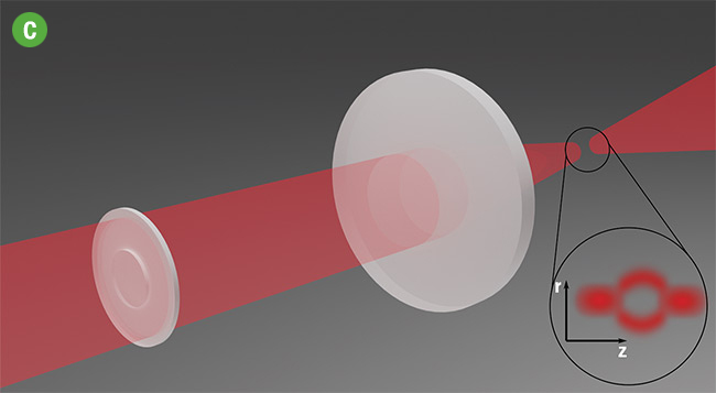
Figure 5. A diffractive axicon-type phase mask for generating Bessel (‘needle’) beams that have an extended zone of high intensity (a). A linear binary phase grating for generating periodic patterns by mask projection (b). A circular phase plate for generating a modified axial focus geometry (for example, zero intensity in the center of the focus) (c). Courtesy of IFNANO.
This technique has resulted in average surface roughness measuring Ra ≈ 3 nm. Subsequent high-temperature treatment leads to a complete oxidation of the remaining layer to highly transparent SiO2. The scanning electron microscope images in Figures 2a and 2b show the sharp edges and smooth surfaces enabled by this method.
Multistep phase elements
The back-side ablation of a single SiOx film only allows the production of two-step elements. The efficiency in a certain diffraction order is, however, significantly higher for multilevel elements. For the fabrication of multistep elements, a structured element is coated with additional SiOx films and subsequently structured after each coating process3. After this, the whole stack is converted into SiO2 during the oxidation step. Using this fabrication method, diffractive phase elements, such as a three-step linear phase grating, have demonstrated a diffraction efficiency of more than 60% in the +1 diffraction order. This compares with 40% for the two-step variant. Efficiency can be increased by adding a higher number of steps through further coating and structuring steps. With four levels (Figure 2b), diffraction efficiency can exceed 80%, and, again, a surface roughness of Ra ≈ 3 nm is achieved on the individual steps.
Applications
Phase masks made of fused silica are suitable for laser materials processing. Their high transparency and the associated high damage threshold make them applicable for high-power processes that would damage or destroy metal-fabricated or chrome-on-quartz masks.
Two-step phase masks are used as diffractive beamsplitters to generate periodic structures by interference structuring (Figure 3). If any intensity in the zero order and in higher orders is blocked, then 80% of the laser energy can be applied to the workpiece by superimposing the two symmetric first orders. If this superposition is achieved by optically imaging the phase mask onto the workpiece surface, very good intensity contrast can be obtained even when using excimer lasers with limited spatial coherence. Lenses, doublets, or — for applications requiring high structure resolution — reflective Schwarzschild lenses can be used as imaging optics with these masks. Structure periods in the order of 1 µm, such as for the diffractive marking of surfaces, require mask periods of several 10 µm at reduction ratios from 10 to 25×.
Figure 3 displays a grating topography on glass fabricated with a single laser pulse at 193 nm by means of the demagnifying projection of a phase mask. In this case, an 80-nm height modulation with a 600-nm period was obtained. Such patterning can enable the diffractive marking of surfaces to create an iridescent label or quick-response (QR) code (Figure 4). Two-dimensionally structured phase masks are also used for the parallel laser drilling of hole patterns4.
Periodic circular phase masks act as diffractive axicons for generating Bessel beams (Figure 5a). The laterally small but axially extended focus spot that they produce is ideal for specific laser microdrilling applications. The optimized design of such radial gratings allows suppression of intensity in the side lobes of the generated ring lobes. Radial gratings can be used to fabricate annular structures through single-pulse material ablation5.
One-dimensional phase gratings (Figure 5b) are also used for structured illumination to increase the resolution in microscopy6. In a nanoscopic method called molecular nanoscale live imaging
with sectioning ability (MoNaLISA), phase masks with a 25-µm period help to generate periodic beam patterns for off-switching the fluorescent signal7. MoNaLISA permits fast, high-resolution image recording of comparatively large sample volumes at low light intensities.
Innovative fabrication methods based on
applying, laser structuring, and oxidizing SiOx coatings over fused silica substrates enable volume production of a class of phase masks with optical surface qualities that are superior to those achieved by laser ablation of the substrate itself.
Circular phase plates fabricated via the methods described (Figure 5c) are effective for creating special focus geometries, such as those required in stimulated emission depletion (STED) microscopy. 3D STED nanoscopy systems combine a vortex phase plate with a binary pi-shift phase plate to enhance both lateral and axial resolutions8. This way the intensity distribution in the focus of the STED beam is optimized in all three dimensions.
The high transparency of fused silica across a wide spectral range, combined with its excellent thermal and chemical properties, make it a versatile material
for phase masks. Innovative fabrication
methods based on applying, laser structuring, and oxidizing SiOx coatings over fused silica substrates enable volume production of a class of phase masks
with optical surface qualities that are superior to those achieved by laser ablation of the substrate itself. The higher performance of such phase masks is
offering broader options for applications in laser materials processing, beam shaping, and microscopy.
Meet the authors
Jörg Meinertz is a senior researcher at the Institute for Nanophotonics Göttingen
(IFNANO), where his main research interests are diffractive optics and excimer laser
materials processing of glass. He studied
physics at the University of Bremen in
Germany; email: [email protected].
Lukas Janos Richter is a doctoral student at the University of Göttingen. He is studying silicon photonics in the nanostructure
technology group at IFNANO; email: [email protected].
Clemens M. Beckmann is a doctoral candidate at the University of Göttingen. He is working on the figuring of optical surfaces in the nanostructure technology group at IFNANO; email: [email protected].
Jürgen Ihlemann is head of the nanostructure technology group at IFNANO; email: [email protected].
References
1. G. Hass and C.D. Salzberg (1954). Optical properties of silicon monoxide in the
wavelength region from 0.24 to 14.0
microns. J Opt Soc Am, Vol. 44, p. 181.
2. T. Fricke-Begemann et al. (2014). Silicon suboxide (SiOx): laser processing and
applications. Appl Phys A, Vol. 117, p. 13.
3. L.J. Richter et al. (2018). Laser processing
of silicon suboxide for the fabrication of multilevel fused silica diffractive phase elements. J Laser Micro/Nanoeng, Vol. 13, p. 249.
4. R. Karstens et al. (2016). Fabrication of 250-nm-hole arrays in glass and fused silica by UV laser ablation. Opt Laser Technol, Vol. 83, p. 16.
5. S. Hasegawa et al. (2018). Diffraction-
limited ring beam generated by radial
grating. OSA Continuum, Vol. 1, p. 283.
6. A. Chmyrov et al. (2013). Nanoscopy
with more than 100,000 ‘doughnuts.’
Nat Methods, Vol. 10, p. 737.
7. L.A. Masullo et al. (2018). Enhanced photon collection enables four dimensional
fluorescence nanoscopy of living systems. Nat Commun, Vol. 9, p. 3281.
8. D. Wildanger et al. (2009). A compact
STED microscope providing 3D nanoscale resolution. J Microsc, Vol. 236, p. 35.