Glass-based chips meet the performance and cost requirements of photon-based quantum technologies where semiconductor materials come up short.
HENNING SCHRÖDER AND WOJCIECH LEWOCZKO-ADAMCZYK, FRAUNHOFER INSTITUTE FOR RELIABILITY AND MICROINTEGRATION IZM
Currently, research on quantum technologies is enjoying a gold rush in funding. Recently published roadmaps provide researchers, industry, and funders with an outlook of what to expect from such research. The documents underscore the technology’s significant potential and some of the steps necessary to translate quantum technologies from laboratory curiosities into something that is ready for mass production.
The fabrication of quantum devices on wafers or panels using established technologies is an essential part of this research. The Quantum Photonics Roadmap from OSA Industry Development Associates (OIDA, now known as Optica corporate membership), for example, sees wafer-scale integration as a more general technological milestone that would enable progress across multiple applications.
Challenges
Most quantum technologies are based on photonics, and they therefore require systems for generating, manipulating, and detecting photons. Developing such systems becomes highly challenging because most quantum processes rely on single photons.
Today’s internet fiber connections rely on streams or packets of photons to transmit data. In these systems, a single photon doesn’t matter much. This is not the case with quantum technologies, in which photons usually represent quantum states.
Quantum states are continuous and not comparable with traditional dual-state bits. Each photon is therefore precious. Yet many are lost and, consequently, the transmission rate of quantum states is often very low.
Generating single photons seems easy if a laser beam is attenuated until only one photon is left. But this approach does not provide single photons on demand. Alternatively, parametric downconversion can generate pairs of photons, though it is an inefficient process.
The transport of single photons is even more challenging, in comparison, because the allowable loss budget is very small. As a result, photonic transport materials must have extremely low absorption, and every interface should be optimized for low losses as well.
Notably, amplification is usually inappropriate for the photonic signals in quantum systems because a quantum state cannot be read out without destroying it. The state thus cannot be amplified. Under certain conditions, a quantum state can be cloned, but this requires using sophisticated technologies to replicate its exact properties and to retain the safety of quantum communication.
In addition to transmission, detection
presents further challenges in the form of noise that originates from the interfaces between optics and electronics. Along with losses, noise must also be minimized.
These factors comprise the basic physical requirements underlying quantum technology systems. But as soon as a quantum system moves from the research lab into a real-world application, economic demands appear. For example, cooling a quantum detector down to almost 0 K requires complex technology that is ill-suited for the gray box of a quantum-encrypted communications terminal in a government office.
In short, viable quantum technology
solutions must be small, reasonably easy to maintain, and scalable, and their cost per part cannot be extravagant.
Glass-based solutions
Embracing existing technologies — such as those used for integrated telecom or data processing components — is one obvious approach to finding a solution for these challenges (Figure 1). The integration of electro-optical interfaces, for example, has most often been a connection between semiconductor and glass components.
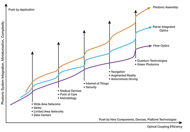
Figure 1. New applications and components lead to higher integrations of photonic systems. Courtesy of Fraunhofer IZM.
Semiconductor materials have allowed for maximum integration of electronic components, while glass materials enable spectrally broad optical transmissions. Silicon has also become a widespread fixture in several photonic domains. But glass remains superior to silicon and other semiconductor materials in several key aspects for photon-based quantum technology. Glass has higher transparency, for example, for the visible and NIR wavelengths that are used in quantum componentry. Additionally, glass can be polished to an extremely smooth surface to reduce any remaining light-scattering effects. Glass is also comparatively cheap.
Single photons can be transmitted in free space or through thin optical fibers, but each coupling process imposes optical losses. This is a well-known issue with telecom components. The use of optical fibers is more beneficial for transmitting photons over long distances, but optical waveguides are superior for integrated solutions. Waveguides can be integrated within inexpensive display glass, which is an excellent base for integrated optical systems.
Fabricating such structures is an established process. At the Fraunhofer Institute for Reliability and Microintegration IZM, for example, ion-exchange processes have been transferred to glass panels measuring as large as 610 × 440 mm. The method allows for parallel processing of large glass substrates, similar to the lithographic processing of silicon wafers.
Over the past decades, we have seen the integration of electronic components achieving near full perfection. Photonic components have followed a similar path of ongoing miniaturization and integration. Currently, micro-optical elements can be placed on minibenches or electro-optical circuit boards. These thin glass platforms serve as scalable optical benches for diverse photon processing tasks.
Figure 2 shows an optical interferometer sensing platform that is ready to be embedded into a larger setup. The in-plane waveguides shown have a diameter of only a few microns and match perfectly the diameter of the in-coupling single-mode fibers. Therefore, no imaging optics are necessary. On the board, the photons require elements for steering and processing. For such purposes, crystals, lenses, or prefabricated periscopes can be inserted and aligned via pick-and-place processes. Grooves for lenses or holes for through vias are precisely made using lithographic techniques.
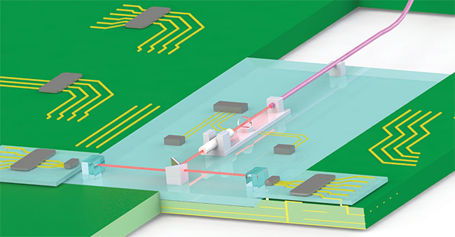
Figure 2. Optical systems, such as an optical interferometric sensing platform, can be integrated into a multifunctional glass board. Courtesy of Fraunhofer IZM.
Beyond optical components, glass also offers great opportunities for combining optical and electric signal processing. Glass can be easily coated with various metals that can be precisely structured with fine lithographic techniques to
provide high-quality guiding lines for direct current and high-frequency microwave signals up to 50 GHz.
Emerging optoelectronic components
The contemplation of photonic components for quantum technology leads to the introduction of components that are rather new for optoelectronics. Integrated vapor cells are one example.
So far, single ions and atoms prove
very beneficial for quantum technology
because they can store and process quantum information. Initial experiments have required a complete laboratory with sophisticated equipment. Substantial miniaturization efforts on the International Space Station, however, have led to a space-qualified setup within a few 19-in. racks.
Glass allows for even further miniaturization of vapor cells down to chip scale. The material exhibits a low outgassing rate and permeability, which makes it
well suited for small, high-vacuum cells. The actual challenge in this application
is sealing the cells under vacuum and
integrating them into more complex
hybrid quantum technology systems.
A new way of coupling fibers to waveguides involves the so-called gradient index surface coupling technique (Figure 3)1. This approach enables the direct
coupling of waveguides on different benches. That is, it allows for the direct coupling of the benches.
Bending waveguides into a third dimension is another challenge that is currently being addressed. In total, these technologies will lead to the operation of an integrated vapor chamber on an optical board, as shown in Figure 3. This, in turn, is the pathway to atomic vapor-based quantum memories and delay lines in quantum networks. It may also serve for other spectroscopic precision measurements.
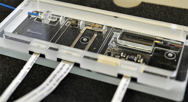
Figure 3. A schematic of an integrated glass optical vapor cell for quantum experiments. GISC: gradient index surface coupling. Courtesy of Fraunhofer IZM.
A glassy future
Glass is a unique material for precision optics. This was true for the optical industry in the 19th century, and it still holds true for the quantum optical developments of the 21st century. Glass has two major benefits. First, it has the required physical properties needed for integrated quantum systems, and, second, the technologies necessary for the industrial processing of glass are available or in an advanced developmental stage.
Integration and miniaturization of optical components will be pivotal for the development of real-world quantum technology devices, and glass shows the potential to serve as a base material for transmitting, processing, and storing quantum information (Figure 4).
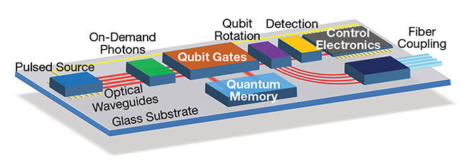
Figure 4. Future integrated quantum optical systems will consist of separate electronic, photonic, or quantum modules. Courtesy of Fraunhofer IZM.
Meet the authors
Henning Schröder is group manager of the Optical Interconnection Technologies Group
at the Fraunhofer Institute for Reliability and
Microintegration IZM in Berlin. His main focus is R&D of optical interconnection technologies for printed circuit boards and photonic modules; email: [email protected].
Wojciech Lewoczko-Adamczyk is a
research fellow at Fraunhofer Institute for
Reliability and Microintegration IZM in Berlin. His main focus is on optical interconnections and photonic packaging; email: [email protected].
Reference
1. J. Schwietering et al. (2020). Integrated optical single-mode waveguide structures in thin glass for flip-chip PIC assembly and fiber coupling. IEEE 70th Electronic Components and Technologies Conference (ECTC), pp. 148-155.