Whether they are aware of it or not, researchers throughout the life sciences heavily rely on optical gratings for Raman spectroscopy, optical coherence tomography, hyperspectral imaging and other applications. New options, such as gratings-on-a-chip, promise to take biophotonics studies to a new level.
DAVID HUANG and BRIAN LIN, II-VI PHOTOP
An optical grating is an optical component with a periodic or quasi-periodic structure. Gratings perform interference of diffracted lights from each grating line to realize specific optical functions, such as the wavelength dispersion, polarization splitting, beam deviation or pulse compression (Figure 1). These components are playing a silent but critical role in a variety of optical systems, such as near-infrared (NIR) spectroscopy, optical coherence tomography (OCT), hyperspectral imaging and Raman spectroscopy (see table), each of which are contributing to major advancements throughout the life sciences. Apart from the traditional applications using gratings as a separated component, there is a trend to integrate gratings into a chip, such as spectrometer-on-a-chip and cytometer-on-a-chip.
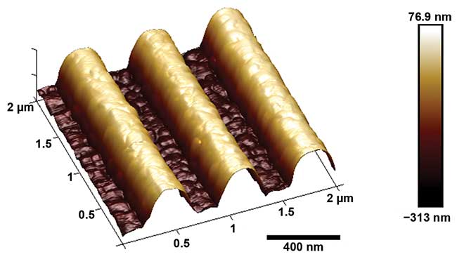
Figure 1. An atomic force microscope (AFM) photo of a holographic photoresist grating (1550 lines/mm). Courtesy of II-VI Photop.
Basic principles
The basic application of a grating is element dispersion (Figure 2). In an open-air environment, its principle is based on this equation:
mλ=(sinα+sinβ)
Here m is the diffraction order, λ is the wavelength, d is the grating period, α is the incident beam angle and β is the diffracted beam angle.
Angular dispersion, resolving power and diffraction efficiency are three key specifications for a grating in a wavelength dispersion application. Other specifications should also be considered for specific applications, such as groove period accuracy, wavefront distortion, light scattering and laser damage threshold.
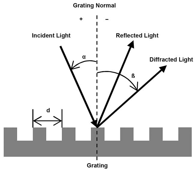
Figure 2. Schematic graph of a diffraction grating (reflection type). Courtesy of II-VI Photop.
The resolving power is determined by diffraction order and groove number. In most cases, the order and angle will be fixed by the system’s design, so the dispersion and resolving power are related to the grating groove density and size, respectively.
Diffraction efficiency (DE) is related to many factors, including grating type, wavelength, material, grating structure and surface status, etc. In most applications, high efficiency is expected. In general, a high-efficiency grating can be calculated by using electromagnetic theory, such as rigorous coupled wave analysis (RCWA). Some empirical approaches for achieving high diffraction efficiency include using blazed grating, minimizing the diffraction orders by optimizing groove density and incident angle, and using a volume phase grating.
Grating fabrication
Fabrication methods and processes have important impacts on grating performance. There are two kinds of gratings that are classified by how they are produced: master and replicated gratings. A master grating is produced by original “writing,” and a replicated grating is copied from a master grating. In most cases, master grating production is more time-consuming and costlier than replicated gratings.
Machine ruling and laser holography (Figure 3) are two traditional methods for making master gratings, which are also known as original gratings. Machine ruling grating covers wider density of grooves. It has an easier — but more costly and time-consuming — production process for blazed gratings, when compared with that for holographic gratings. The laser holography method has higher period accuracy and relative low cost, so it is widely used in commercial master gratings manufacture. A holographic photoresist grating can be further transferred to its substrate by a plasma etching process to produce a blazed grating or deep-etched grating. And further, some gratings such as volume Bragg grating (VBG) and deep-etched grating can be produced by laser holography but cannot be produced by machine ruling due to the lack of groove on the surface for the former, or deep groove for the later. Additionally, new methods have also been developed in recent years. They include scanning beam interference lithography (SBIL); laser, e-beam or ion-beam direct writing; or projection photolithography process. The last method uses a conventional semiconductor process to produce gratings, especially for deep-etched gratings.
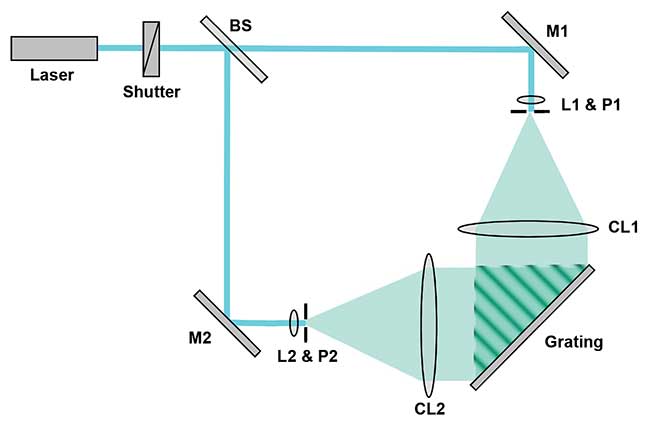
Figure 3. Schematic graph of a recording system for holography grating. Courtesy of II-VI Photop.
Some surface-relief-type gratings, which are only modulated by their surface profile, can act as a master grating. They can be used to produce replicated gratings with groove profiles that are nearly identical to the master’s. The typical replication process begins with release and glue layers that are added between the master grating and replication part. Subsequent steps include curing the glue by heat or UV light and separating them, resulting in the master grating’s groove profile being transferred to the replicated grating’s surface. Volume grating and some deep-etched grating cannot be replicated due to a lack of surface groove and separation difficulty.
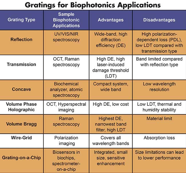
It is important to understand how varying features of different grating types contribute to their value for different applications in the life sciences (see table). Most biochemical analyzers, for example, employ concave grating to simplify the structure and avoid extra stray light from the surface of mirrors or lenses, but plane reflection or transmission gratings could also be used for this application if users carefully handle the stray light. Most Raman spectrometers use a reflection grating, but handheld versions on this technology commonly employ concave and transmission gratings. Descriptions of these types of grating and others follow:
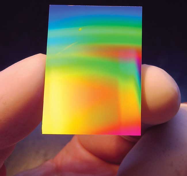
Figure 4. A gold-coated reflection grating (1200 lines/mm). Courtesy of II-VI Photop.
Reflection grating: One of the most widely used gratings in the market. In general, the grating surface is a coated metal layer, such as silver, gold or aluminum, or a multilayer dielectric highly reflective (HR) coating for reflection. When an aluminum-coated grating is used in wavelengths less than around 300 nm, a protective layer, such as magnesium fluoride (MgF2) or silicon dioxide (SiO2), should be coated on the aluminum to prevent its oxidation in air.
Compared with a transmission grating, a typical metal-coated reflection grating has a relatively wide spectral band, especially when it is used in a spectrometer. Due to the reflection grating’s single surface, there are lower light scattering and straying effects. Most reflection gratings can be replicated from a master grating, opening the door for low-cost, mass production (Figure 4).
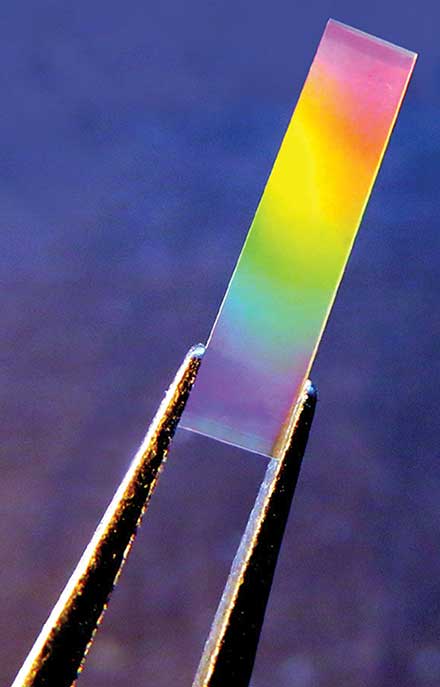
Figure 5. A fused silica transmission grating (966 lines/mm), which is used in optical communication. Courtesy of II-VI Photop.
Transmission grating: A good choice for when high diffraction efficiency is needed in two polarizations. In some high-power applications, transmission gratings are the only option because they have the highest laser damage threshold (LDT). In such cases, the grating should be made of a high LDT substrate, such as fused silica glass, and a high LDT coating. Additionally, it must be a master grating. A common shortcoming of transmission gratings is their backside reflection. This feature causes unwanted stray light and sometimes results in a spectral “ripple” due to multiple reflections between the backside and surfaces. Although an antireflection coating is usually employed, it cannot totally remove all the reflection. To solve this problem, a small wedge is usually made in the grating substrate to separate the backside reflection from the working beam direction (Figure 5).
Figure 6. A concave grating with 430 lines/mm, which is used in biology testing systems. Courtesy of II-VI Photop.
Concave grating: An optical component that combines the function of dispersion and imaging (Figure 6). This combination improves the system’s compactness and working efficiency. The aberration-corrected flat-field concave grating is widely used for color measurement and spectrometry (Figure 7).

Figure 7. An optical path in a typical aberration-corrected flat-field concave grating system. Courtesy of II-VI Photop.
Volume phase holographic (VPH) grating: A type of grating with a diffraction wave that comes from a periodic refractive index modulation in a thick medium. The most commonly used medium is dichromated gelatin (DCG). This grating is recorded by laser holography technology. Due to DCG’s sensitivity to humidity, almost all gratings used in this medium need to be covered and sealed in glass, plastic or another protective material. By optimizing the DCG thickness and refractive index, high diffraction efficiency in two polarizations can be realized in a VPH grating. Due to DCG’s organic makeup, VPH gratings are limited to high-power applications (Figure 8).
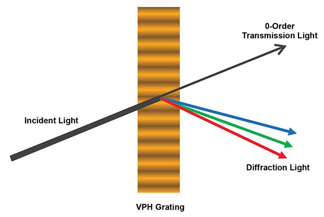
Figure 8. Schematic graph of a volume phase holographic grating. Courtesy of II-VI Photop.
VBG: A grating that incorporates the concept of Bragg diffraction in a crystal in x-ray. A VBG is formed by working in a bulk material that has periodic refractive index distributions. When the Bragg condition is satisfied in a certain direction, the diffraction beam will reach its highest intensity. Compared with the DCG version of VPH, VBGs are thicker — by approximately several millimeters — and most of them are made of glass or crystal. Most commercial VBGs are made of photo-thermo-refractive (PTR) glass, and the grating is recorded by UV laser holography. Although VBG is a kind of grating, in many cases it acts as a narrow band filter. Its band can be lower than 1 nm, which is hard to achieve in a filter with a thin-film coating (Figure 9). A narrow band transmission VBG can act as coupling mirror in a laser cavity to realize the specific narrow line output, which is beneficial to the laser source in a Raman system.
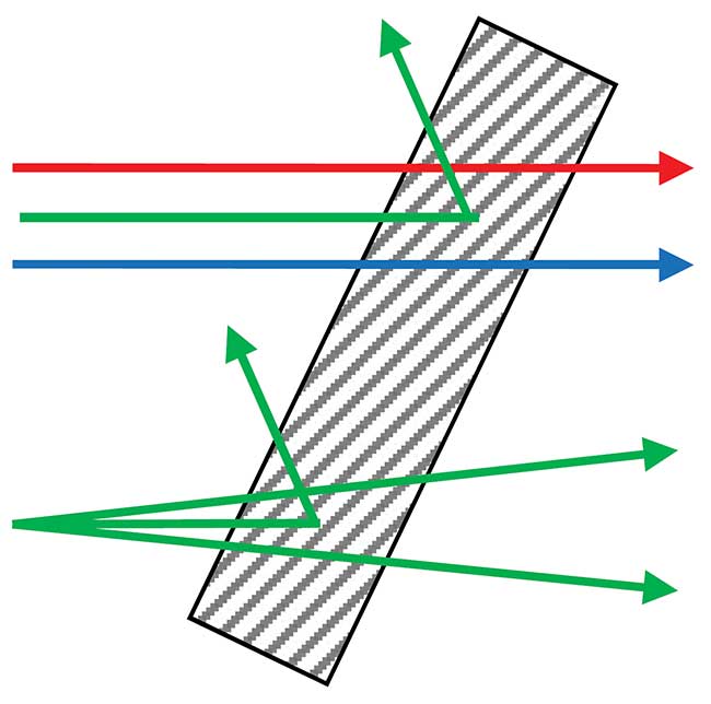
Figure 9. A volume Bragg grating acts as spectral filter and angular filter. Courtesy of II-VI Photop.
Wire-grid grating: Wire-grid gratings feature grating lines that are made of conductive material, all of which are separated by insulation material. Wire-grid gratings primarily act as optical polarizers. This type of polarizer is mainly used in the UV and infrared regions where almost no other materials adequately perform. Illustrative of their uniqueness, wire-grid gratings are also used as a polarizing beam splitter in the visible light region due to their wider incident angular tolerance compared with the thin-film coating components.
Grating-on-a-chip: As the name suggests, a grating-on-a-chip is a grating made on a chip or wafer. In principle, most gratings can be integrated onto a wafer. Optical communication and biophotonics are the two areas that are increasingly integrating a greater amount of functional components on a chip. Arrayed waveguide grating (AWG) and surface plasmon resonance (SPR) grating are two examples of gratings-on-a-chip that are commonly used for optical communication and surface-enhanced Raman systems, respectively.
As a new and continually developing area, the role of the gratings-on-a-chip in biophotonics will only become larger over time. More and more researchers work on the areas of lab-on-a-chip, spectrometer-on-a-chip and cytometry-on-a-chip. Most of them integrate gratings as a dispersion component, mirror, filter or SPR or other sensor.
Meet the authors
David Huang is the senior research and development engineer at II-VI Photop in Fuzhou, China, a subsidiary of II-VI Inc.; email: [email protected]. Brian Lin is the product manager at II-VI Photop in Fuzhou, China; email: [email protected].