YORKTOWN HEIGHTS, NY, March 2, 2009 – In a landmark study in the field of nanoelectronics, IBM Research scientists have announced the development and demonstration of techniques that measure the distribution of energy and heat in powered carbon nanotube devices.
By employing these techniques, IBM researchers have determined how the energy of electrical currents running through nanotubes is converted into heat and dissipated into collective vibrations of the nanotube's atoms, as well as surface vibrations of the substrate beneath it.
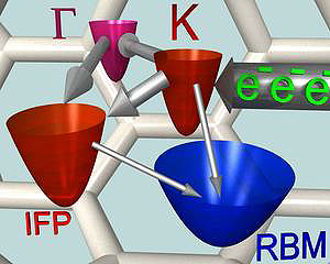
The figure shows an artist's conception of a nanotube being heated (excited) by passing a current of electrons (e-'s) through it. The energetic electrons excite preferentially the mode of vibration of the carbon atoms labeled K. Then the energy flows to other vibrational modes with different rates schematically indicated by the width of the arrows. At the end a non-equilibrium energy distribution is established. Image courtesy of IBM Research.
"The understanding of how heat flows through specific nanotube devices will have important implications on the operation and integration of future carbon-based devices," said Phaedon Avouris, IBM fellow and manager, nanoscale science and technology, IBM Research. "This finding is crucial to creating the nano-thermal management systems that will regulate heat of these devices and is also of fundamental scientific importance."
Carbon nanotubes are tiny molecular tubes about 100,000 times thinner than a human hair and consist of rolled up sheets of carbon hexagons, similar to an atomic scale chicken wire. They are leading candidates as wires and active channels for future computer chips and can be packed thousands of times closer than the components on of standard chips.
For years, scientists have known that carbon nanotube devices get "hot" during operation. However, it was not known how to measure the effects and understand the transfer of energy within the device structures and how that heat was dissipated.
IBM scientists studied a single, semiconducting carbon nanotube incorporated as the active channel of a transistor. The ultimate sensitivity of resonant light scattering detection, in combination with electrical transport measurements, allowed them to monitor the changes in the optical properties of the nanotube while an electrical current flowed through it. The researchers used these changes as "thermometers" to probe how the energy of the electrical current was dissipated among the different modes of vibrational motion of the atoms of forming the nanotube and those of the supporting substrate.
Using this method, IBM researchers were able to map the population of the principal vibrational states of the nanotube and determine the energy dissipation pathways of the transistor under functioning conditions. The scientists found a non-thermal-equilibrium (non-statistical) distribution between different vibrational modes with the high energy modes heated to "effective temperatures" in excess of 1000 degrees Celsius, while low energy modes remained relatively cold, around 400 degrees Celsius, for the same electrical power level. Most importantly, they found that the electrical transport in the device and the heat transport from the nanotube to its substrate were strongly affected by an efficient, direct-coupling mechanism between the charge carriers in the nanotube and atomic lattice vibrations at the surface of the insulating substrate beneath it. Compared to the case of conventional bulk semiconductor devices, the energy transport through this dissipation channel was found to be greatly enhanced.
The results challenge a long-lasting paradigm in condensed matter physics and physical chemistry by demonstrating that the equilibration of energy among vibrational states in one-dimensional (line-like) materials, such as carbon nanotubes, can be significantly inhibited.
Furthermore, the observation of non-equilibrium vibrational distributions in electrically pumped low-dimensional systems opens up a new scientific quest: How do physical and chemical properties of such systems differ under equilibrium and non-equilibrium vibrational excitation?
For more information, visit: www.ibm.com/research