GAITHERSBURG, Md., Sept. 5, 2008 – “It's the physics,” explained Andras Vladar, of the National Institute of Standards and Technology’s (NIST) Nanoscale-Metrology Group, when referring to the new helium ion microscope.
NIST researchers announced that this new technology uses helium ions to generate the signal that is used to image extremely small objects, which is similar to the scanning electron microscope (SEM) that was first introduced in the 1960s.
Now, they are looking to further improve measurement accuracy at the nanoscale because according to the group, nanoscale is critical for setting standards and improving production in the semiconductor and nanomanufacturing industries. 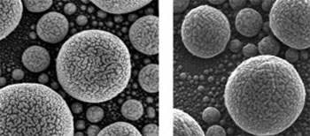
In-depth look: An image of gold atoms on tin from a state-of-the-art scanning electron microscope (left) has relatively poor depth of field. Only parts of the image are in sharp focus. By contrast, the entire image from a helium ion microscope image (right) is sharp and clear. (Photo: NIST)
Ironically, although helium ions are far larger than electrons, they can provide higher resolution images with higher contrast. The depth of field is much better with the new technology too, so more of the image is in focus.
“Ions have larger mass and shorter wavelength than electrons, so they can be better for imaging,” said Vladar.
According to Vladar, the images appear almost three-dimensional, revealing details smaller than a nanometer - the distance spanned by only three atoms in the silicon crystal.
NIST is working to understand the imaging mechanisms of this new technology. The clearest advantage of the helium ion microscope is that the images show the actual edge of a sample better than the SEM, which is critical in precision manufacturing.
“Meeting critical dimensions by knowing where an edge is in high-tech manufacturing can mean the difference of hundreds of dollars per piece,” explained Michael Postek, chief of the NIST Precision Engineering Division and the nanomanufacturing program manager.
Semiconductor manufacturers have multi-million dollar SEMs all along their production lines to help control their microchip manufacturing processes.
NIST received the first-ever commercial helium ion microscope, called Orion, from Carl Zeiss Inc. last summer as part of a cooperative research and development agreement. Researchers are test-piloting it in NIST’s Advanced Measurement Laboratory (AML), one of the most environmentally stable research facilities in the world. Carefully controlled for vibration, humidity and temperature changes, AML labs are optimal sites to test new microscope technology, said the researchers.
“What we are learning goes directly back to the manufacturers to improve their products, which allows NIST and the industry to obtain the most precise measurements possible,” explained Postek. “We are transferring NIST technology and sharing our research with the semiconductor industry trade organization, Sematech.”
One such NIST contribution is “fast imaging,” a technique Vladar developed to obtain sharper images. A combination of vibrations at the nanoscale and taking images at high resolutions left certain images fuzzy, similar to what happens when taking a picture of a moving object with a slow shutter speed. Instead of collecting the signal slowly and getting a fuzzy image, the NIST technique collects many images as fast as possible and merges them using a clever algorithm to reduce the fuzziness and result in a much sharper image.
Zeiss has recently replaced the original Orion with the first-ever Orion Plus, which incorporates many of NIST’s suggestions in its design, including an improved cooling system for the helium source for improved imaging.
For more information, visit: www.nist.gov