Optical coating capabilities expand with a new reactive sputtering process.
Michael Walls and Des Gibson, Applied Multilayers Ltd.
Sputtering processes for thin-film deposition are naturally energetic and generally do not require additional heat input to generate good morphology. As a result, sputtering is a suitable deposition technique for heat-sensitive substrates such as polymers, as well as for traditional substrates such as glass and semiconductors. Sputtering also produces coatings that are dense and spectrally stable when exposed to water vapor in the atmosphere.
Reactive sputtering using simple metal or alloy targets offers a number of advantages for high-throughput optical coating applications. Using metal rather than compound targets allows pulsed DC power to be applied, which results in much higher deposition rates than with traditional radio-frequency power. Using linear magnetrons to heat long, narrow metal targets provides uniform coating over large areas. The technique also makes the technology scalable in terms of both batch coatings and industrial-scale systems. The latter involves in-line systems in which substrates are inserted into a load lock at one end of a multistage deposition system and emerge at the other end into an exit chamber with a multilayer coating applied.
A new form of reactive sputtering uses unbalanced magnetrons of opposite polarity to confine a reactive plasma in the closed magnetic field between them. This field produces an extremely high plasma density without applying bias voltages to the substrate carrier. The result is an energy of deposition that is close to ideal as well as coatings that have low losses and that are supersmooth (although the morphology can be controlled if required). Thickness control to ±1 percent is achieved using time only, and the process is maintained simply by monitoring target voltage. This flexible process already has been used to deposit high-quality thin films of metals, metal oxides, metal nitrides, metal oxynitrides, metal carbides and transmitting conducting oxides.
Applied Multilayers Ltd. developed the closed-field magnetron process for its range of batch systems but recently has licensed the technology for industrial-scale use in in-line and roll-to-roll formats. The process can be used for making high-volume antireflection coatings on plastic, for electrochromic coatings, for polymer organic LED (p-OLED) displays and for thin-film photovoltaics.
Closed field
In the closed-field configuration, adjacent magnetrons are arranged with magnets of opposite polarity, producing a magnetic “bottle” that supports an intense, chemically activating plasma in which the oxidation (or some other chosen reaction) takes place. As a result, the oxidation of the metal is extremely efficient and complete and leads to low absorption. Because no separate ion or plasma source is required, the process is simple, reliable and less expensive than previous ones. Metal targets are used with pulsed DC power supplies to avoid charge buildup and arcing. Oxidation at the target surface is simply controlled using target voltage with feedback to the oxygen gas admission. Using simple metal targets reduces coating costs and dramatically increases deposition rates.
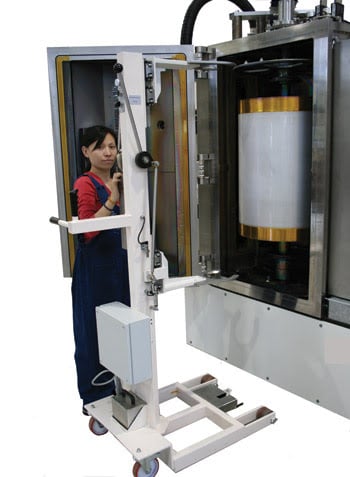
Figure 1. The CFM850 system uses a 0.5-m retractable cylindrical drum for substrates and 1-m linear magnetrons for deposition. In this case, the machine is being used to deposit a six-layer high-performance antireflection coating on a 1.4 × 0.6-m polycarbonate sheet.
The midsize batch system shown in Figure 1 uses the closed-field configuration with thin-film deposition provided by up to six separate linear magnetrons, 1 m in length. The substrates are mounted on a 0.5-m-diameter vertical drum, which rotates at 50 rpm during coating. The system usually is fitted with a Meissner trap to remove water vapor and to minimize pump downtimes. Magnetrons can be used in tandem to increase rate, or they can be used to increase the number of materials available.
The process is low temperature and low stress, which makes it particularly suitable for use with plastic substrates. It is already being used with CR39 plastic and polycarbonate to apply antireflection coatings to spectacle lenses with controlled residual reflection color and mirror coatings for sunwear lenses. It can be used at high rates while maintaining the substrate temperature below 60 °C and also is used to apply antireflection and complex electrochromic coatings onto thin polycarbonate sheets (Figure 2).
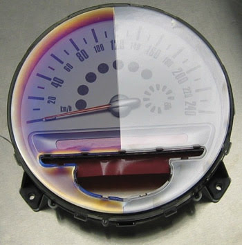
Figure 2. A high-performance antireflection coating has been deposited on one side of this plastic automotive instrument display window.
Durability is important when applying optical coatings to plastic substrates, and here the closed-field process also has important advantages over previous methods. For example, for Si3N4 deposition, a closed-field deposited film was measured to have a fivefold reduction in compressive stress (–120 MPa) compared with an equivalent film deposited using plasma-enhanced chemical vapor deposition. Low stress is also important in deposition of passivation or encapsulation layers for OLED displays or thin-film photovoltaics.
In addition, the process allows silicon oxynitride to be deposited simply by controlling the flow of the two reactive gases (oxygen and nitrogen). The oxynitride system provides a range of refractive indices, which are controlled by the O:N ratio.
Tuning the ratio can provide optimal antireflection properties. This is particularly important for thin-film photovoltaics because it provides a simple way of improving light collection and efficiency.
The quality of thin films of transmitting conducting oxides such as indium tin oxide (ITO) is vital to the performance of a range of new products in high-growth markets such as electrochromics and OLED displays, and also thin-film photovoltaics based on either CdTe or copper indium gallium selenide absorbers. In many of the most exciting applications, these devices are being applied to polymer substrates, so it is vital that the processes provide excellent electrical, optical and mechanical properties while maintaining low-temperature deposition. The closed-field process produces ITO films that provide electrical conductivity of 10 ohm/sq with high optical transmission with a thickness of 360 nm deposited at room temperature with no postannealing. Moreover, the deposited ITO thin films are supersmooth.
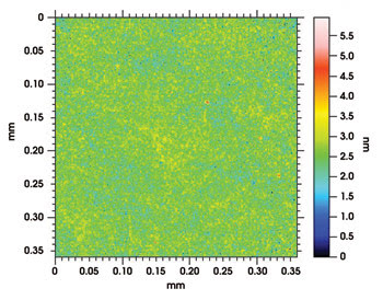
Figure 3. A coherence correlation interferometry image reveals the metrology of a 365-nm ITO film deposited at room temperature. The color scale shows the maximum height difference across the 0.35-mm-square sample area. The measured rms roughness from this area is Sq = 0.453 nm. Data courtesy of Ametek’s Taylor Hobson Ltd.
Surface metrology studies using coherence correlation interferometry show that the rms roughness of a 360-nm film typically is less than 0.5 nm, even though the deposition rate exceeds 5 Å/s. Supersmooth ITO films are particularly desirable for OLED display devices. The reason why the process works so well is not completely understood but is probably the result of the high plasma density generated by the closed field, which does not depend on deliberately biasing the substrates, as is necessary when using a conventional ion source. Rough or porous films (as required for electrochromics or dye solar cells) can be obtained by increasing ion energy by appropriately biasing the substrate during deposition.
Besides deposition of metal oxides and metal nitrides, the closed-field process also is advantageous for high-volume deposition of protected silver and aluminum reflectors on plastic automotive parts.
The sputtering technique can perform room-temperature deposition of low-stress carbon-based films, which are used as durable optical coatings for the mid- and thermal-infrared spectral regions. Two examples of materials used for such films are germanium carbide and diamondlike carbon, which can be used for low-cost high-volume thermal imaging systems for a variety of commercial safety and security applications. Other applications include single- and dual-band durable antireflection coatings for infrared targeting, navigation and surveillance systems.
These materials are deposited by sputtering germanium and carbon, respectively, in a hydrocarbon-reactive gas. The refractive index of germanium carbide can be tuned from 4 (pure germanium) to 1.8 (stoichiometric germanium carbide). The films’ very low (<1 percent) hydrogen incorporation minimizes optical absorption, so they pass standard military salt fog, severe abrasion and humidity/temperature cycle tests for external surface coatings. Closed-field sputtered germanium carbide and diamondlike carbon currently are being applied as durable external surface antireflection coatings on a wide range of infrared materials, including Ge, ZnS and ZnSe.
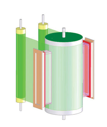
Figure 4. This model illustrates how the closed-field configuration can be adapted for roll-to-roll thin-film deposition onto a polymer sheet or metal foils. The magnetrons facing the large roller are constructed so as to be of opposite magnetic polarity.
Applied Multilayers has developed the closed-field magnetron process for a standard range of batch systems with drum diameters from 25 to 75 mm and linear magnetrons with lengths from 40 cm to 1.2 m. However, the process is equally applicable to continuous in-line or roll-to-roll industrial-scale processing because the basic geometry of the system can be maintained in these formats. Figure 4 shows how the process is adapted for the roll-to-roll format, where two magnetrons of opposite polarity are used in a configuration exactly as used in the equivalent batch system. This approach should allow this process to be quickly adopted in a wide range of new high-throughput markets for thin-film technology.
Meet the authors
Michael Walls is the chairman and a founder of Applied Multilayers Ltd. in Coalville and is a visiting professor of physics at Loughborough University, both in the UK; e-mail: [email protected].
Des Gibson is the CEO and a founder of Applied Multilayers Ltd.; e-mail: [email protected].