As ChatGPT makes it to the evening news, less spectacular AI routines are helping optical and optoelectronic system manufacturers to reduce costs and increase productivity.
ERIK BECKERT, FRAUNHOFER IOF, AND ANDREAS THOSS, CONTRIBUTING EDITOR
Many trends in the manufacture of photonic
systems are well known: miniaturize and integrate components, scale-up batch sizes, and, increasingly, expand automated and sustainable manufacturing. At the same time, quality control remains a priority but faces ever more challenges, such as zero-defect production or full traceability. Maintaining these goals calls for a “detect/predict/prevent/repair” approach based on comprehensive sensor networks that monitor every step in the production
chain as well as complex software to make use of the data that these networks produce. Artificial intelligence is critical to success.
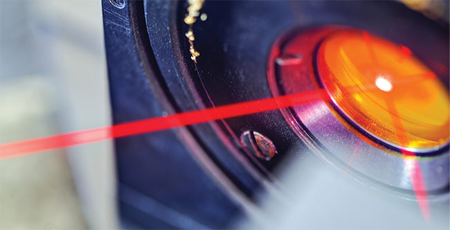
Laser deflection allows the monitoring of mirror alignment during production. Courtesy of iStock.com/vladimir_n.
With this in mind, a group of European companies and research institutions joined forces to develop “a holistic framework applicable both to new and existing manufacturing lines of optoelectronics to achieve flexibility, zero-defect production, and sustainability,” as stated in their project plan (Table 1). Funded through Europe’s Horizon 2020 program, the so-called iQonic project aims to explore sensing and process chains for increased quality, reconfigurability, and recyclability of manufacturing optoelectronics.
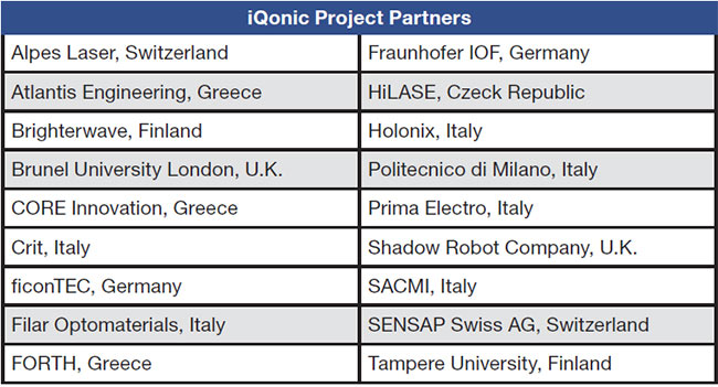

Figure 1. The wafer image (left) was normalized to a rectangular grid before evaluation (right). See Reference 1. Courtesy of Alpes Lasers and Sensap.
The project defines zero-defect manufacturing as an approach to prevent defective photonic components from reaching the customer. All efforts, consequently, are focused on identifying defective parts as early as possible within the manufacturing process and supply chain. Each of the many steps within this process are costly and, thus, time and money can be saved through early identification and elimination of potentially defective parts.
According to a scientific publication by the project’s researchers, the group chose zero-defect manufacturing over other quality improvement approaches, such as Six Sigma or Lean Six Sigma1. Their decision was due to the unique characteristics of photonic manufacturing processes, which are characterized by the production of small to medium quantities, the individualization of high-value products, and long value chains with heterogeneous sequences of manufacturing processes and technologies. These characteristics not only result in a significant amount of production-related data but also necessitate the interpretation of this data using a combination of statistical- and knowledge-based techniques.
Industrial use cases
When the project commenced in autumn 2022, the general approach was to collect data on various points of the photonics manufacturing chain in different application cases and to consider how team
members could use that data to improve manufacturing performance to get closer to attaining zero-defect production. Within this framework, the partners worked on use cases at four participating
companies, including Alpes Lasers’ production of quantum cascade lasers (QCLs); Brighterwave’s high-volume production of optoelectronic multicomponent modules; Filar Optomaterials’ manufacture of synthetic crystals from raw materials; and Prima Electron’s production of fiber-coupled, high-power laser diode modules.
The approach to the project goal
implemented similar practices to those applied by the Industrial Internet of Things or Industry 4.0; smart sensors and software were employed to monitor and enhance manufacturing processes. More
specifically, the data from a quality control framework was used either to guide
development of further quality measures (as measured by accepted versus rejected
parts) or to start repair processes. The data can also be used to establish measures to prevent defects early in the process that can help increase quality, with the final goal of zero-defect-production and zero waste. All four use cases in the project successfully implemented this manufacturing approach.
Predicting laser malfunctions
The use case implemented by Alpes
Lasers to produce QCLs exemplifies many of the typical challenges in the manufacture of optoelectronic systems. The production of QCLs starts with sophisticated semiconductor processing techniques to bring the laser structures onto a wafer. This step is followed by a large number of complex manufacturing and measurement steps to complete the laser module.
Although many single measurements deliver data along this manufacturing chain, the final accept/reject decision depends on whether the laser achieves
an expected output power at a certain wavelength at a certain temperature.
Importantly, at various points in the process, problems can occur that will contribute to malfunctions in the finished laser, resulting in a failed component.
Evidently, the criterion that determines an accept/reject decision cannot be tested in early production steps. Nevertheless, certain sensor data can help predict the malfunction of the finished module early in production.
For example, if a microscopic image shows missing grating structures, the part will not produce the correct radiation. The objective of the project was to use sensor data and machine learning to establish a relationship between image data and the final laser output. With this approach, it is possible to predict which parts will exhibit output power below the required threshold earlier in the process. Further, production operators could make such decisions via a user interface.
Finding grating defects
The researchers found that for the manufacturing of QCLs, visual and microscope inspections for defect detection were enough to collect data for the intended decision process.
The visual inspection process essentially aims to find defects in the laser’s grating structure. The process from data acquisition to decision-making can be broken down into four steps.
The first two steps include image acquisition and correction for perspective and lens distortion, followed by a device mapping process in which the grating structure on the wafer is identified in a device map. The low-resolution image shown in Figure 1 provides information about the quality of a grating. It should
be noted that the grating is embedded into the top layer of the wafer and no longer visible after subsequent processing steps.
The second step requires reconstruction of the wafer map and the creation of a
raster image. The registration of structures makes use of corresponding point pairs on the wafer. With a trained segmentation model, several classes of defects can be identified, and a new wafer image with colored markings of the defect is created and presented to the operator (Figure 2).
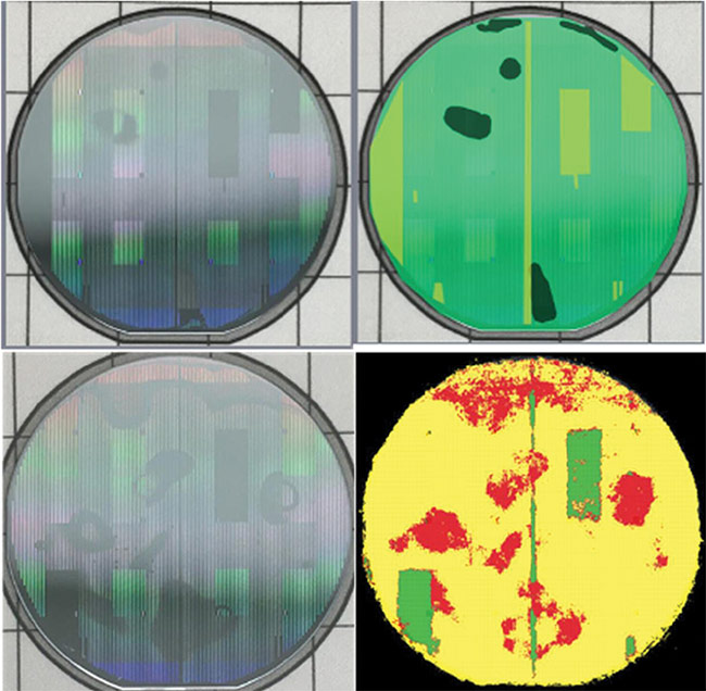
Figure 2. Top row: Original wafer image (left) and annotated image (right). Bottom row: Original wafer image (left) and corresponding defect detection result (right). See Reference 1. Courtesy of Alpes Lasers and CORE.
The third step is to evaluate the device for defects by first preparing a training data set that distinguishes past devices according to whether they failed or not, and then training the machine learning software to extrapolate characteristics of either device category to identify different classes of defect. Once they are trained, these models offer precise recommendations for identifying potential defects within the image.
In the fourth and final step, the decision support system combines the outputs of the previous steps and visually presents the results to the operator (Figure 3).
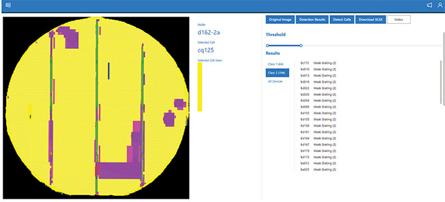
Figure 3. A machine learning-driven decision support system presents the evaluation results to the user. See Reference 1. Courtesy of Alpes Lasers and Atlantis Engineering.
Failure detection with a microscope
Usually, the wafers are inspected for defects using a microscope with 5× magnification. This is enough to identify every single laser chip and to decipher those that were impacted by a defect. For a 2-in. wafer, 400 microscope images are stitched together. The resulting amalgamation comprises 20,000 × 20,000 pixels with color information. Obviously, automating the evaluation process for defect detection can save enormous amounts of time.
Again, the image must be mapped first
to allow for effective defect recognition.
In this case, a complex set of rotation,
translation, and scale processes are
applied to deliver a final map for regis-tration. Once the mapping process is complete, the defect detection algorithm is applied to the adjusted image. Defect detection uses image processing techniques such as template matching, thresholding, morphological operations, and edge detection. The results of the tests are used for a “pass” or “fail” decision on every component. The software implementation for the Alpes Lasers’ use case consists of subservices developed by technology providers. These subservices communicate via a common bus implemented through a higher-level communication middleware (HLCM). The HLCM acts as an orchestrator, following a microservice architecture, and facilitates the flow of information in both low- and high-resolution wafer images. Data distribution is achieved through an MQTT broker (a machine-to-machine network protocol), in which images are published by the manufacturer, aggregated, and relayed through different microservices responsible for mapping the wafer devices, detecting defects, and providing outputs to the decision support system (DSS) for easy identification of problematic devices by manufacturer engineers. The DSS is the user interface in which the results of both evaluation steps are presented to the operator (Figure 3).
The outcome
The system implemented in the Alpes Lasers’ use case was tested for hundreds of lasers from several wafers. Using a combination of the two-defect detection schemes, it demonstrated that a laser categorized as a “pass” with no grating defects has a 6× higher chance of lasing at a specific frequency compared to a laser categorized as “fail” with a full grating defect.
As one end user of the iQonic zero-
defect-manufacturing approach noted, this is already a huge benefit to Alpes Lasers’ QCL manufacturing process, because defective components will be spared its subsequent, long, and expensive value-adding manufacturing sequences, and will not compromise yields1.
This new monitoring tool for the life cycle of optoelectronic devices uses both image processing as well as deep learning algorithms.
Defect identification has been automated by using two image-based
defect detection pipelines that use low-resolution grating pictures and high-resolution surface scan images, respectively. All acquired data is labeled with additional defect-type classifications, resulting in device maintenance guidance for the optoelectronic engineer.
Similar systems have been developed for the iQonic project’s other three use cases as well2. They also use data input from devices embedded in a ficonTEC machine, for example, or from a chemical sensor. All use cases have shown that compiling and analyzing data that is collected early in the manufacturing process can enable accurate predictions of the final product’s performance. This allows a rerouting of components in the early stages of the manufacturing chain, allowing those components to be either recycled, repaired, or removed before additional processing steps are wasted on them.
The project commenced in September
2022, and participants, such as the Fraunhofer Institute for Applied Optics and Precision Engineering, continue to improve upon the technology.
Meet the authors
Erik Beckert received a diploma in precision engineering in 1997 and a doctorate in optoelectronics system integration in 2005, both from Technical University of Ilmenau, Germany. Since 2001, he has been with the Fraunhofer Institute for Applied Optics and Precision Engineering (IOF) in Jena, Germany, where he has been head of the Opto-mechatronical Components and Systems department since 2020.
Andreas Thoss, Ph.D., is a laser physicist, founder of THOSS Media, and a contributing editor to Photonics Spectra. He has been writing and editing technical texts, with a focus on the field of photonics, for two decades.
References
1. G.P. Moustris et al. (2022). Defect detection
on optoelectronical devices to assist
decision making: a real industry 4.0 case study. Front Manuf Technol, Vol 2, https://doi.org/10.3389/fmtec.2022.946452, CC BY https://creativecommons.org/licenses/by/4.0/.
2. Zero defect manufacturing approaches for optoelectronics and photonics (Oct. 6, 2022), final project presentation webinar, www.iqonic-h2020.eu/2022/10/06/zero-defect-manufacturing-approaches-for-optoelectronics-and-photonics-the-iqonic-project-within-horizon2020/.