
Hyperspectral Method Adds Speed, Accuracy to Wafer Inspection
A high-throughput metrology technique for semiconductor manufacturing, developed by Samsung Electronics, combines spectroscopy and imaging to measure in-cell uniformity (ICU) and in-wafer uniformity (IWU) of semiconductor devices used in high-volume manufacturing.
The approach, called line-scan hyperspectral imaging (LHSI), measures semiconductor structures with speed, high spatial resolution, and high spectral resolution. It could provide a way to ensure accurate uniformity down to the finest equipment details — the critical dimensions — in semiconductor structures.
In the LHSI system, a narrow rectangular beam, or line scan, illuminates the surface of the wafer. The reflected beam is relayed to a hyperspectral module comprising an arrangement of mirrors, slits, gratings, and cameras. The gratings spatially decompose the incoming beam into its constituent frequencies, which are then captured by cameras optimized for different spectral ranges.
The cameras acquire the spectral information of each vertical “pixel” of the rectangular beam in one shot. This allows a large amount of data to be generated quickly, which speeds the measurement of critical dimensions. Compared to standard optical critical dimension (OCD) systems, the LHSI system is able to provide more detailed information about the structural variations in cells and wafers because it is able to obtain and analyze large amounts of spectral data.
“Our system enables the simultaneous collection of massive amounts of spectral and spatial information with an extremely large field of view of 13 by 0.6 mm2,” Myungjun Lee, head of the Inspection Solution Group at Samsung Electronics, said. “Additionally, our method has an improved throughput of up to 10,000 times compared to the standard OCD method.”
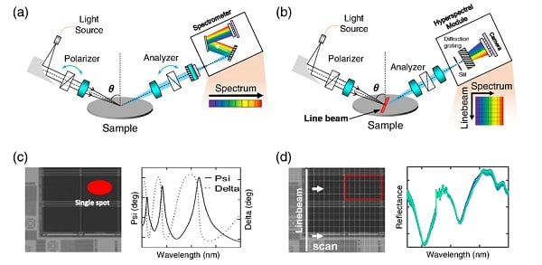
(a, c): The OCD spectroscopy approach. Though practical, it has limited spatial and spectral resolution and long scan times. (b, d): The LHSI approach developed by the research team, with a shorter scanning time and much higher spatial and spectral resolution. Each square in the grid shown in (d) corresponds to an observed 'pixel.' Courtesy of Yoon et al., doi 10.1117/1.JMM.21.2.021209.
The key difference between OCD spectrometry and LHSI is the way in which the surface of the semiconductor is scanned. OCD focuses a beam of light to produce a bright spot on the wafer. The reflected light is captured by a spectrometer and analyzed. Due to the large spot size, OCD systems have low spatial resolution.
The LHSI system offers a spatial resolution of 5 μm and a spectral resolution of 0.25 nm in the broad wavelength region covering 350 to 1100 nm. Using LHSI at this resolution, the researchers were able to clearly observe fine details on semiconductor devices. The researchers demonstrated that the LHSI system can significantly increase the throughput of scatterometric measurements and provide both high spatial and spectral resolution, enabling the precise monitoring of ICU and IWU.

Existing metrology methods for measuring critical dimension uniformity in cells, chips, and wafers cannot offer speed and accuracy and reliability — instead, they offer a trade-off between these capabilities. Transmission electron microscopy and atomic force microscopy, for example, offer high spatial resolution, but their scanning speeds are too slow to use in high-speed manufacturing.
To the best the researchers’ knowledge, they are the first research group to demonstrate a line-scan-based HSI metrology technique for semiconductor applications.
“We believe that there is currently no technology other than LHSI that can be used to analyze CD uniformity at such high levels of throughput and resolution,” Lee said. “It could be the tool we need to overcome current measurement limitations in the field of high-volume semiconductor manufacturing.”
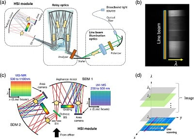
LHSI optics methodology. (a): Schematic illustration of LHSI optics methodology. A wafer is scanned by a broadband line beam with dimensions of 13 × 1 mm2, and the reflected signal is dispersed and detected by a 2D area camera. (b): The raw image detected by the camera. The broadband line beam is dispersed along the wavelength axis. (c): HSI module, which consists of two SDMs. The reflected signal is cropped by a slit to enhance the imaging performance and increase the spectral resolution. Two SDMs and a detector are used applied to cover the 350- to 1100-nm broadband without spectral error. (d): 3D data cube generated by the LHSI system. Specifically, it is generated by stacking the line beam image for each scan position. Courtesy of Yoon et al., doi 10.1117/1.JMM.21.2.021209.
As device sizes continue to shrink, uniformity of critical dimension has become of growing concern. A modest fluctuation in critical dimension, which may not have affected the previous generation of semiconductor devices, could reduce yield in the current generation of semiconductors. Demand for chips continues to increase, making high-speed, high-throughput manufacturing even more important.
Although LHSI will require a more stable light source, higher sensitivity cameras, and higher precision optics, it has the potential to be adopted for high-throughput ICU and IWU measurements of semiconductor devices used in high-volume manufacturing. Further improvements to LHSI technology could help accelerate semiconductor development and fabrication processes, reducing their cost and enhancing the performance of electronic devices.
The research was published in the Journal of Micro/Nanopatterning, Materials, and Metrology (www.doi.org/10.1117/1.JMM.21.2.021209).
/Buyers_Guide/Samsung_Electronics_Co_Ltd/c24654