Applications for intensified CCD cameras range from miniature electronic night vision to low-light imaging of cellular interactions.
Mike Buchin, Stanford Photonics Inc.
Originally developed to enhance night vision in military applications, image intensifiers combined with improved CCD imaging sensors emerged as serious contenders for low-light scientific imaging applications in the early 1990s. Today many intensified CCD cameras employ the same CCD sensor found in cooled scientific cameras, the goal being to combine a high-gain amplifier with a good low-light image sensor.
A typical intensifier has three key elements. The first stage is a flat, circular photocathode formed from various semiconductor materials within which photon energy is converted to electrons. Electrons emitted from its rear surface travel tens of microns across an electric field to a two-dimensional microchannel plate, which, by virtue of a high-voltage differential acting across it, can dramatically amplify the number of electrons passing through it (gain multiplications of 10,000 to 80,000 are typical). These then impinge on a phosphorescent output screen on one side of a fiber optic faceplate, forming an amplified image that can be visualized on the faceplate. With standard night-vision goggles, that is the extent of the intensifier components.
In this 9-oz intensified CCD camera (1.6 × 2 × 3.75 in.), direct fiber optic coupling between intensifier tube and image sensor results in a five- to tenfold increase in sensitivity compared with intensified CCD cameras using relay optics.
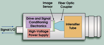
In many cases, the value of an image is enhanced dramatically if it can be converted to electronic form for analysis, display and/or presentation. To create an electronic representation of the intensifier output, a CCD or CMOS image sensor can be attached to the rear of the tube, most effectively through the use of another fiber optic element that conducts the amplified image directly to each pixel. Fiber optic bonding allows attachment to sensors with pixel sizes down to 5 μm, but commercial technology more often uses 6.4-μm, 1.4-megapixel formats (Sony XX285) or 9-μm VGA resolutions (640 × 480 pixels).
Read noise, dark current
The goal of image amplification is to boost the electronic rendition of the original scene to well above the imaging device’s read-noise and dark-current limits. To detect a signal in the presence of random noise, it must be three to five times above the rms or noise average, depending on the detection quality threshold.
For a device with a combined rms level of 10 electrons, one would need to convert at least 30 photons with 100 percent quantum efficiency to “see” these photons in the electronic image. Things get even worse if the quantum efficiency is lower. With the high light gains afforded by the image intensifier, single photons can generate hundreds of electrons in each pixel, so the read-noise and dark-current contributions no longer interfere with detection, even at high frame rates and high pixel clock frequencies.
In cooled scientific cameras, however, manufacturers often must chill devices to temperatures well below 0 °C to reduce dark current of the random noise floor. This still leaves the read-noise element in place. To reduce this, it is usually necessary to slow down the pixel clock frequency, which proportionally reduces image readout speed. This is why the most extreme scientific-grade cameras, with read-noise levels in the single digits, may use pixel clock speeds as low as 100 kHz, leading to 10-second readout times for 1-megapixel images. Reductions are less dramatic for the most common cooled scientific cameras; e.g., five- to tenfold.
A competitively priced cooled device can come within a factor of 20 to 50 in terms of low-light detection capability relative to an intensified CCD camera, but speeds are typically slower; e.g., five instead of 30 fps for comparable resolutions. That may be adequate when end users aren’t dealing with dynamic-motion events or biological transients, or when they can illuminate the sample enough to get a fluorescence signal to adequate levels for detection. Because photons are multiplied in the stage before the final detector, an intensified CCD camera can run at lower light levels and higher speeds without running into the read-noise/dark-current limit.
More recent competition in the area of low-light imaging comes from cameras using electron-multiplying CCD technologies. These devices attempt to produce the same effect as an intensifier within the CCD structure, by introducing a small increase in gain for each step in a shift process that moves the charge from each pixel through and out of the chip for subsequent processing and digitization. On-chip gains of up to 1000 can be achieved in this manner.
Unlike standard CCDs, these sensors must be chilled to between –45 and –70 °C because the residual dark current is multiplied along with any real signal that is converted in the origin pixel. Although the theoretical specifications for electron-multiplying CCD products claim noise levels of ±1 electron rms, other factors, such as clock-induced noise, make it difficult to reach this level in practice.
Current field tests and feedback from independent evaluators indicate that these still do not quite match the low-light performance of intensified CCD cameras when at the photon limit. One possible reason is that, at maximum gains, images from these cameras show some measurable noise component in every pixel. On the other hand, at 30 fps, an intensified CCD running at a light gain of 40,000 will present dark counts (thermally generated at the cathode) in less than 5 percent of the pixels in the image, which can be a significant advantage when photon flux levels are low. With the latest cooled photocathode cameras, it is possible to generate gains approaching a million and to demonstrate “zero dark count” images at 30 fps.
In surveillance applications, intensified CCDs retain significant advantages in power, size and cost, in part because electron-multiplying CCDs require Peltier cooling with associated vacuum-sealed front ends to reach the low light limits. Peltier coolers require many watts and large thermal masses for heat dissipation to function most efficiently. These thermal masses can become target beacons to a thermal imaging countersurveillance system.
Although CMOS sensors are beginning to find their way into intensified platforms, they do not yet match CCDs in low-light performance. However, their on-sensor functional integration and low power combine with features such as dynamic range extension to make CMOS the Holy Grail for the night-vision developer.
Meet the author
Mike Buchin is president of Stanford Photonics Inc. in Palo Alto, Calif.; e-mail: [email protected].