Event-based imaging, which eliminates saturation, and sensors that detect in sub-400-nm UV or 400- to 1700-nm visible and SWIR ranges are among notable recent sensor advancements.
HANK HOGAN, CONTRIBUTING EDITOR
There’s arguably never been a more exciting time for the development of image sensors, with notable achievements in 3D imaging, event-based sensing, and nonvisible imaging. Recent innovations have focused on pixel architecture and sensor circuitry, while other advancements have involved the use of new materials, greater data processing within the
sensor itself, and improvements in manufacturing that increase performance and cut cost.

In a stacked CMOS image sensor, the light-sensitive pixels (upper layer) are fabricated on one chip, and the transistor logic (lower layer) is made on a second chip. The two chips are bonded together to make the image sensor. Courtesy of Sony Semiconductor Solutions.
These innovations help to explain why the industrial segment is growing faster than the overall image sensor market. Florian Domengie, senior marketing and technology analyst at Yole Intelligence, part of the Yole Group, put the overall growth of the market at 6.7% versus more than 9% for industrial applications. The industrial market segment stands at $0.7 billion today, with Yole projecting it will reach $1.2 billion by 2027.
The dominant player is Sony Semiconductor Solutions, which has about
a 50% share of the industrial image sensor market, according to Seiji Aoyama, a leader in industrial sensor
marketing and promotion. Sony’s recent product activities involve event-based imaging, a technology in which the sensor captures only changes, such as those from movement. Event detection can be performed using
software, but this approach involves shipping data to a processor with enough storage and power to do a pixel-by-pixel comparison.
“That requires some more processing time and energy, whereas with event-based vision, that happens natively on the chip,” said Matthew Dyson, a senior technology analyst at IDTechEx.
Another benefit of event-based imaging, Dyson said, is larger dynamic range. Pixels discharge when they’ve collected a certain number of photons, thereby eliminating the saturation that occurs when a scene has some very bright points in a dark background. An everyday example of this is a streetlight at night on an otherwise dark road.
Other recent announcements by Sony involve sensors that image sub-400-nm UV light or 400- to 1700-nm visible and SWIR light. Objects that are difficult to detect, such as stones or other contaminants in black beans, become easier to spot with sensors that operate outside the visible.
Another announcement involves global shutter technology that enables all the pixels on a sensor to acquire the image during the same time period and then it effectively reads out the pixels all at once.
“In addition to our imaging function, we are also working on [incorporating a] sensing function with image sensors,” Aoyama said while discussing enhancements to Sony products.
Implementing sensing capability and data extraction on a chip requires
putting additional circuitry into a sensor, increasing its size. Sony’s technology, however, makes it possible to shrink the pixel size, according to Aoyama.
The company offers stacked architectures. In a two-layer version of this approach, Sony fabricates the analog pixel section on one chip and the logic-processing circuitry on a second. Sony then bonds and connects the two chips together into one final stacked image sensor. This technique reduces the size of the image sensor while allowing optimization of each separate component.
Event-based sensing
Sony collaborated with Prophesee, an event-based sensor technology startup, to develop a stacked, event-based image sensor. The result of the partnership, unveiled at the February 2020 International Solid-State Circuits Conference, was the smallest pixel size in the industry at that time and the highest performance in terms of dynamic range.
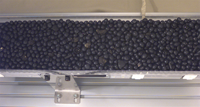
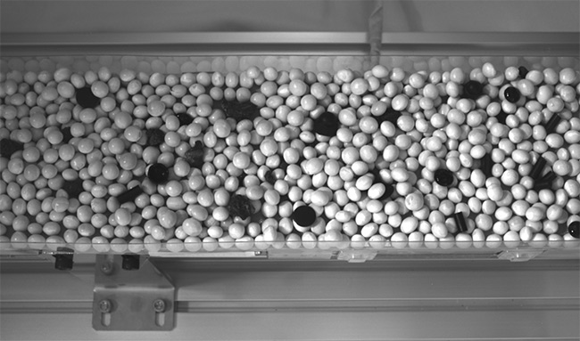
Contaminant detection has been made easier thanks to image sensor innovations. The properties of shortwave infrared (SWIR) imaging make it possible to distinguish between food products, such as black beans, and black-colored contaminants. A visible light environment (top) and a SWIR environment (bottom). Courtesy of Sony Semiconductor Solutions.
Event-based sensing systems offer several advantages in an industrial setting and for automation applications, including greater efficiency in conveying information and a larger dynamic range, according to Prophesee CEO Luca Verre. They also offer increased speed, with event-based systems reacting in microseconds, effectively equivalent to a 10,000-fps traditional image sensor.
Event-based sensors require
additional circuitry at the pixel level, however. They must independently detect contrast changes or motion and activate. Implementing this capability takes space, which makes the pixel larger. Advanced manufacturing that stacks sensor pixel and logic components atop one another allows the pixels to be smaller and the resolution to therefore be higher than it otherwise would be.
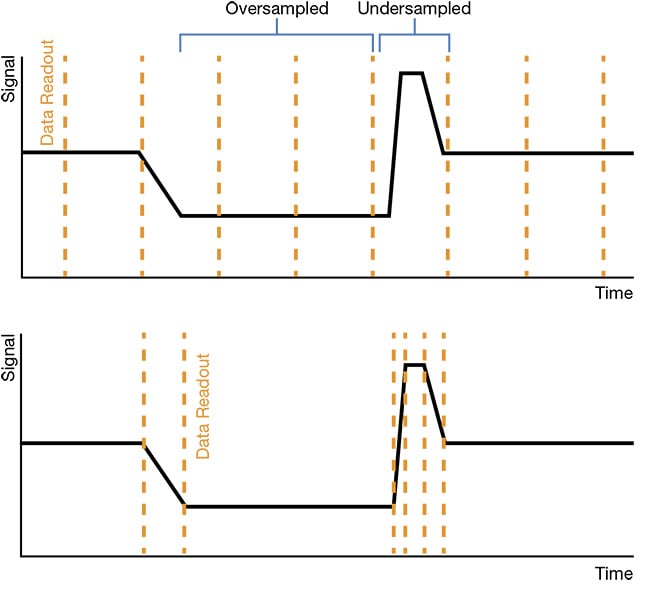
In traditional image sensing, the sensor collects data and provides it at regular intervals, which leads to missing information if an object moves or other image changes occur between collection times (top). In event-based sensing, the sensor reacts to changes in a scene and does not collect data when it does not detect changes or motion (bottom). Courtesy of IDTechEx.
An event-based system reacts in microseconds, effectively equivalent to a 10,000-fps traditional image sensor.
When asked about industrial and automation uses cases, Verre pointed to vibration measurements performed on a pump or other piece of machinery. The moving parts of a machine in operation cause slight shifts in the location of spots on its surface, which are events that a sensor detects.
“We can monitor these events over time and compute a vibration frequency,” Verre said.
Such vibration monitoring, in turn, plays a role in preventive maintenance because a machine’s characteristic vibration changes long before one of its parts fails. Detecting changes and drifts in vibrations can therefore lead to greater uptime and — more importantly, from a cost perspective — help to eliminate unplanned downtime.
Event-based sensing also aids process control. For example, observing the spatter from laser welding or ablation with a high-speed, low-latency, event-based sensor yields data about the material addition or removal process. This information is useful for process control.
Global shutter is another image sensor innovation benefiting industrial applications and automation. In a global shutter, an in-pixel memory element stores the signal after it is captured by the photodiode. In a rolling shutter, a competing approach, readout moves line by line from one side of the sensor
array to the other. Global shutter technology is particularly important when objects move, with faster moving objects benefiting more because of the reduction in blur.
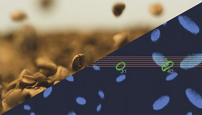

Event-based sensing can be used to capture particle size, such as in food (top), or it can be used for the high-speed counting of objects such as pills (bottom). Courtesy of Prophesee.
Devang Patel, marketing director for emerging IoT at OMNIVISION, said rolling shutter technology can handle moving objects by using a fast enough readout speed, such as one suitable for a 200-plus-fps output. However, this approach leads to a shorter exposure time, which can affect image quality and the amount of data that can be extracted from an image.
On the other hand, global shutter technology needs more transistors and storage at the pixel level than a rolling shutter does, leading to bigger pixels and greater cost. Determining which approach is best is application dependent, Patel said.
Thicker silicon
Patel said some applications need color in the visible and sensitivity in the near-IR, at either 850 or 940 nm. One challenge is that the quantum efficiency for CMOS, which is 80% in the visible, falls off steeply in the near-IR, dropping
below 10% at longer wavelengths. OMNIVISION addressed this challenge through pixel-level innovations that made the silicon a bit thicker, enlarged the size of the photodiode, added scattering layers below the color filter, and put a reflector on the side of a deep trench to improve near-IR light gathering. The result was an improvement in efficiency at 850 nm from 20% to 60%, and at
940 nm from 8% to 40%.
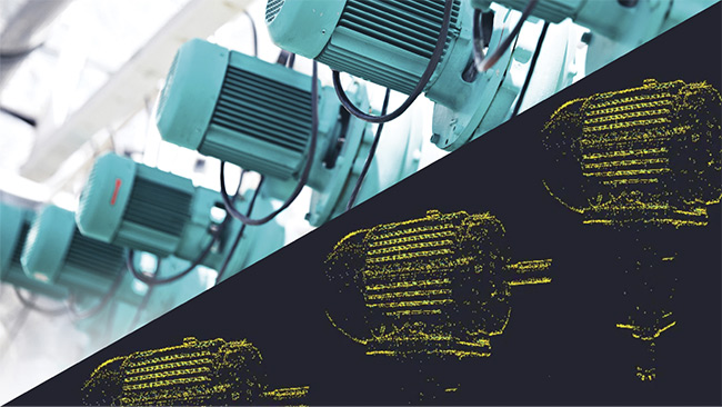
Event-based imaging detects machine vibrations, an indicator of machine health that can be used to determine when to perform preventive maintenance. Courtesy of Prophesee.
“The benefit is you can see objects in no light with an IR source. Second, you don’t need very strong illumination,” Patel said of these innovations. “So that helps with the power budget and heat. If you want to keep the same power, the same intensity, the same number of LEDs, you will see much longer distances.”
A crossover exists between the technology used for industrial image sensors and that used for other applications. For instance, stacking technology became a mature process in image sensors
used for consumer applications before
it was applied to industrial sensors.
Axel Clouet, a Yole Intelligence technology and market analyst, said little overlap exists between consumer and industrial image sensors. The former tend to have smaller pixels, while the latter tend to have larger pixels and a higher average selling price per part — two characteristics of image sensors used in the automotive and security markets as well.
But the consumer market is much larger than the industrial, automotive,
and security markets, combined. The size and volume that the consumer
market demands creates a link
between the different markets.
“In the long term, though, the consumer area is a volume-driving market. So, it helps technologies to get mature and decrease in terms of manufacturing cost,” Clouet said.