Doug Malchow, Sensors Unlimited
Researchers and manufacturers of concentrated photovoltaic (CPV) cells have recently achieved record solar cell conversion efficiencies of 41 percent by overlaying three semiconductor layers. Careful selection of both the materials and the chemical structures used within the cell will result in matching the absorbance of each layer to the sun’s spectrum. When this occurs, each layer contributes equal amounts of electrical current to the cell’s output.
Because the layers are photodiode junctions connected in series, the maximum current output of the cell is limited by the output of the lowest-performing layer. It’s important to ensure that all three layers work efficiently; otherwise, the current from the strong layers will dissipate power into a weak layer. The multijunction cells are usually assembled at the focal point of light concentrators, which are designed to focus the equivalent of 500 suns onto an area measuring 1 cm2. This then generates amps of current.
It is vital for cell fabricators, solar concentrator integrators and solar farm installers to inspect individual cells before incurring the expense of final assembly into large concentrator structures. Fortunately, multispectral electroluminescence imaging can be used to separately inspect each layer’s junction uniformity and relative output.
Typical multijunction CPV cells, as indicated above, are small, yet they generate a lot of current, so the collection lines and bus bars must be robust but not so large as to block the sunlight from the cell surface. As shown in Figures 1-3, the collection lines are only 10 µm wide on 100-µm centers.
Dust particles or defects in the various layers also can seriously affect energy collection. Consequently, high-resolution inspection is a requirement for quality control. Current technology for short-wave infrared area cameras provides video graphics array resolution of 640 columns by 512 rows, while short-wave infrared line-scan cameras permit imaging of 1024 pixels.
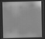
Figure 1. This electroluminescence image of a multijunction cell was acquired with an InGaAs 1024-pixel line-scan camera array without filtering. The image was cropped to 880 columns x 773 rows. The horizontal line pattern consists of 10-µm lines on 100-µm centers.
Thus, the highest-resolution imaging can be obtained by scanning the wider linear array over the small CPV cell. The line-scan camera is mounted on microscope optics, and the line acquisition is synchronized with the motorized stage movement. This permits ultrahigh-resolution imaging by taking several passes, each offset to the side to image a different portion of the cell.
Figures 1-3 show how imaging electroluminescence with several filters is used to find nonuniformities, cracks and defects in the cell layers. These images are of one type of multijunction cell, composed of gallium indium phosphide (GaInP) and gallium indium arsenide (GaInAs) layers on a germanium substrate. ImageXpert of Nashua, N.H., acquired the photos in a single pass using its wafer inspection system with a Goodrich high-speed, indium gallium arsenide (InGaAs) digital line-scan camera.
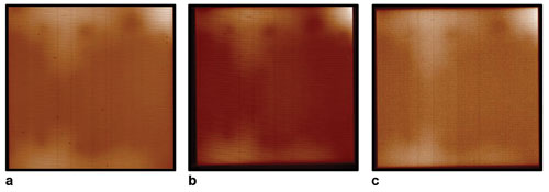
Figure 2. (a) An electroluminescence image of the same cell as in Figure 1 was taken with an 800-nm short-pass filter in front of the lens to capture only the 700-nm emission from the top GaInP layer. Note the number of dark spots apparent. The image is displayed with a warm-scale false color plot generated by the Goodrich Sensors Unlimited Image Analysis program to bring out details within the dynamic range of the image. This helps make the dark spots visible. (b) This electroluminescence image was taken with a combination of 800-nm long-pass and 1250-nm short-pass filters to isolate the electroluminescence emission at 920 nm from the middle layer of the GaInAs film. (c) The same cell is shown in this electroluminescence image taken with a 1250-nm long-pass filter to capture the emissions from the germanium substrate, which are mostly at wavelengths longer than 1550 nm. All electroluminescence images (Figures 1, 2a, 2b and 2c) are courtesy of, and were acquired by, ImageXpert.
The black-and-white image (Figure 1) was acquired without a wavelength filter other than the camera’s natural response from 700 to 1680 nm. The other three electroluminescence images (Figure 2) were acquired through filters that isolate the emissions of each layer. The top layer (Figure 2a), emitting around 700 nm, shows a number of dark spots that are not visible in the other images, indicating that the defects causing them are relatively transparent to the longer wavelengths. However, some of the dark spots are noticeable in all of the images. These are likely caused by dust or digs on the top surface, which will block all wavelengths from reaching the camera.
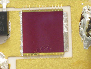
Figure 3. Shown is a color photo of a multijunction CPV device that is glowing red because the forward bias is driving the top layer to emit at 700 nm. This particular cell has physical damage to the fine collector lines in its lower part, but it is otherwise the same type as imaged in Figures 1 and 2.
As demonstrated, new inspection tools using electroluminescence – and short-wave infrared – imaging systems are helping to meet the increasing demands for efficient and affordable multijunction CPV cell inspection. To replace fossil fuels with solar cells, manufacturers must deliver high quality and optimal output power, and imperfections such as nonuniformity must be detected early in the production process so that costs can be curtailed and the goal of efficient, renewable energy production can be achieved.
Meet the author
Doug Malchow is business development manager of industrial products at Sensors Unlimited (part of Goodrich ISR Systems) in Princeton, N.J.; e-mail: [email protected].