Yuliya Akulova, John Gheorma and Mike Larson, JDSU
Indium phosphide-based photonic integrated circuits (PICs) eliminate optical loss between different functional elements and use high-efficiency optical modulators to enhance performance. They are indispensable in the development of the small-form-factor, high-power-efficiency pluggable (SFP+) transceivers operating at 10 and 100 Gb/s for optical communications.
Widespread adoption of smartphones, tablets, video content and cloud computing continue to fuel rapid growth in optical network traffic. The increasing demand for transmission capacity delivered with low cost and high energy efficiency is driving innovations in both short- and long-reach optical communications applications.
To overcome fiber transmission impairments at higher modulation rates – and to overcome speed limitations of optical and electrical components – new optical transmitter architectures increasingly rely on transmission components with multiple functional elements (lasers, modulators, power splitters/combiners and wavelength multiplexers). For example, 100-Gb/s optical transmitter architecture for the local area network applications adopted by IEEE in 2010,1 100GBASE-LR4 (long reach) and ER4 (extended reach), combines 25-Gb/s modulation with multiplexing four wavelengths into one single-mode fiber. In the metro and long-haul space, demand for increased line-card density and reduced power dissipation is being supported by 10-Gb/s SFP+ (small-form-factor pluggable) transceivers, either operating at a fixed wavelength or tunable over the C-band. This application utilizes a traditional on-off keying (OOK) modulation format and requires an externally modulated laser to meet the requirements for dispersion tolerance. In addition, starting from 40 Gb/s, long-haul and metropolitan-area telecom applications adopted advanced modulation formats, including polarization multiplexing and multi-level quadrature amplitude modulation.2 A polarization-multiplexed advanced-modulation format transmitter requires a laser and two quadrature modulators, typically realized using a nested Mach-Zehnder (MZ) architecture.
The requirements for increased optical transmission speed and complexity combined with stringent constraints on cost, size and power dissipation can be met only by implementing photonic integration to replace several packaged components with one. Photonic integration can be categorized into two types: Hybrid integration co-packages several active optical components that are optically coupled using micro-optics or planar lightwave circuits; monolithic integration combines multiple active and passive optical elements fabricated on a single semiconductor chip to form a PIC. In practice, a combination of hybrid and monolithic integration is frequently used.
InP PIC technology
The primary functional sections of an optical transmitter PIC include light-generation and amplification sections, modulation and passive optical routing sections. Fortunately, fundamental material properties of indium phosphide (InP) and related quaternary indium gallium arsenide phosphide (InGaAsP) and indium aluminum gallium arsenide (InAlGaAs) compounds enable all required functionalities. The compelling advantages and possibility of monolithic photonic integration in InP have been recognized from the early 1980s, and multiple approaches to integrate regions with different absorption/gain properties together along a single waveguide have been developed and are widely used in InP PIC fabrication (see the tutorial paper3 and references therein).
Among various integration technologies, butt-joint integration enables flexibility in the design optimization of each PIC section with minimum transition length. In most cases, all functional sections of the PIC are p-i-n heterostructure diodes, with i-waveguide core containing bulk quaternary material or multiquantum well (MQW) layers. In the butt-joint integration technique, the laser gain layer stack is typically grown first on a planar substrate and then protected with a dielectric mask where it is required in the PIC. The exposed gain layers are then etched away, and the layers for the next functional section are grown by metallorganic chemical vapor deposition (MOCVD). This process can be repeated several times to produce an optimized layer stack for each PIC section. The primary advantage of the butt-joint integration technology is that the layer stack and doping can be changed abruptly, so optimum design can be independently selected for each of the functional sections.
Specifically, the optimized laser gain layer stack design typically contains narrow compressively strained MQWs with the effective bandgap detuning of ~25 nm relative to the target operating wavelength. The optimized modulator design typically requires wider quantum wells and larger detuning, as described below. The primary requirement for the passive waveguide section, used for light routing and/or multiplexing, is low optical-propagation loss. This is accomplished by even larger bandgap detuning and reduced doping to eliminate free-carrier-absorption loss. The typical optical loss at the butt-joint transition between the sections does not exceed 0.1 dB, provided that the optical mode matching is ensured in the design and fabrication process. This low-loss integration is essential for high-power-efficiency components. In contrast to the monolithic approach, co-packaging a laser and modulator chips fabricated on the separated wafers typically introduces 2- to 4-dB loss. This loss needs to be balanced by higher laser drive current resulting in higher power consumption.
High-performance tunable lasers
Monolithically integrated C-band tunable lasers based on carrier injection into sampled grating-distributed Bragg reflectors (SGDBRs) have been known for many years4 and are in high-volume production. 100G coherent transmission places a new requirement for narrow (<500 kHz) spectral linewidth on these lasers. This is difficult to achieve due to the increased absorption and resulting broadened linewidth at higher values of tuning current. This challenge can be overcome through the use of thermally tuned gratings with monolithically fabricated microheaters, whereby the tunable mirrors are thermally isolated from the substrate to enable very low thermal power dissipation.5 Figure 1 shows a cross section of such a chip. Linewidth below 300 kHz and output power in excess of 16 dBm can be achieved across the C-band with less than 100 mW of tuning power, representing a tenfold improvement in tuning efficiency compared with nonisolated mirror designs.
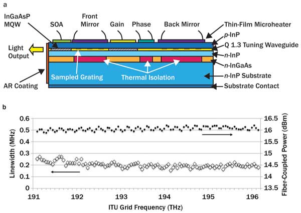
Figure 1. (a) Schematic of a monolithic widely tunable SGDBR laser utilizing high-efficiency thermal index tuning design. (b) Output power and linewidth for 102 calibrated channels on a 50-GHz ITU grid.
High-efficiency InP modulators
As the baud rate and the number of modulated elements for a single optical transmitter go up, so does the power dissipated by the drivers. For a given baud rate, the driver power dissipation can be significantly reduced if the modulation voltage is lowered, making high-efficiency modulators a key enabling component for pluggable transceiver modules at 100 Gb/s for both short- and long-reach applications.
High-efficiency InP electroabsorption (EA) and electro-optic MZ modulators in InP material systems fundamentally rely on the quantum-confined Stark effect, which produces redshift of the MQW absorption edge when reverse-bias voltage is applied across p-i-n modulator structure. The redshift of the absorption edge also results in a refractive index change. For both types of modulators, the modulation efficiency can be enhanced by proper choice of the MQW stack.
Figure 2 shows an example of the absorption-edge shift in InAlGaAs MQW material and the desired offset between the unbiased absorption edge and the operating wavelength. For both modulators, a smaller offset results in improved modulation efficiency at the expense of additional optical loss. Modulator design optimization also includes the device length, depletion region width and electrode configuration to achieve desired modulation bandwidth. EA modulators typically are short (<200 µm) and use lumped electrode designs; MZs are longer (>1 mm) and implemented with traveling-wave electrodes. In both cases, the modulation bandwidth requirements for 25-Gbaud operation can be easily met.
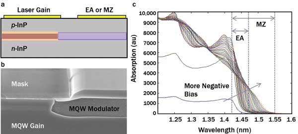
Figure 2. (a) Schematic cross section of the integrated laser and electro-absorption or electro-optic modulator. (b) Scanning electron microscope image of the butt-joint transition. (c) Absorption spectra of InAlGaAs MQW (multiquantum well) modulator, measured for multiple reverse bias voltages applied across p-i-n structure.
Figure 3 presents spectral and modulation characteristics of a 4 × 25-Gb/s transmitter optical subassembly (TOSA) based on EA modulators integrated with distributed-feedback (DFB) lasers. The TOSA footprint is 19 × 6.6 × 5.5 mm, enabling CFP2/CFP4 and QSFP28 transceiver modules that meet 100GBASE–LR4/ER4 performance requirements developed for 10- and 40-km-reach applications. The mask margin of 40 percent and the RF extinction ratio in excess of 5 dB and 9 dB are demonstrated with the modulation voltage of 1.2 and 1.5 V, respectively. Such low requirements on the drive voltage ensure compatibility with low-power-dissipation modulator drivers, and improve the power budget of the transceivers.
EA modulators can deliver excellent performance at high bit rates in the wavelength range of minimum fiber dispersion, but they suffer from excess absorption loss when negative chirp is required to counteract fiber dispersion in the C-band. Unlike the 1.55-µm EA modulators, the optimization of the InP MZs for low drive voltage imposes a less stringent trade-off between insertion loss, modulation efficiency, extinction ratio and chirp characteristics because the transient chirp and extinction ratio of p-i-n InP MZ modulators are primarily determined by the interferometer design (the splitting ratio of the two multimode interference sections and the differential phase shift between two arms).
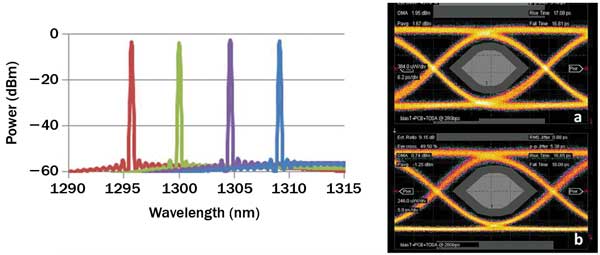
Figure 3. Spectral characteristics of the electro-absorption modulated laser-based 100GBASE–LR4/ER4 TOSA. Optical spectrum analyzer resolution bandwidth = 0.1 nm, and eye diagrams measured at 28 Gb/s PRBS 231-1 for 100G TOSA calibrated for (a) RF ER >5 dB with peak-to-peak voltage (Vpp) = 1.2 V and (b) RF ER >9 dB with Vpp = 1.5 V. Mask margin is >40 percent in both cases.
Additional advantages of the DFB-MZ architecture over typical EML (electro-absorptive modulated laser)-based solutions for TDM (time-division multiplexing) and DWDM (dense wavelength-division multiplexing) SFP+ include lower on-chip power dissipation – because no photocurrent is generated in the modulator section – and high manufacturing tolerances that allow the requirements for bandgap detuning control to be significantly relaxed. Also, because of larger detuning, MZ modulators offer superior characteristics over a wide wavelength range and can be used in monolithic, widely tunable transmitters. Figure 3 shows the image of an SGDBR laser monolithically integrated with a semiconductor optical amplifier and MZ modulator. The C-band tunable transmitter chip footprint is only 0.4 × 4 mm, and the required modulation voltage in differential drive configuration is less than 1.6 Vpp per side. For single-wavelength transmitter chips comprising a DFB laser and MZ modulator, the modulation voltage can be further reduced to below 1 Vpp per side by optimizing laser-modulator detuning. The combination of low TOSA power dissipation and low drive voltage enables low power dissipation TDM and DWDM SFP+ and T-SFP+ transceivers (<1.5 W) for 80-km reach
applications.
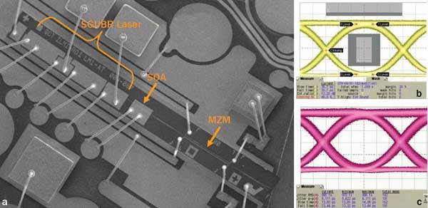
Figure 4. (a) Scanning electron microscope image of an optical transmitter PIC comprising a C-band tunable SGDBR laser, a semiconductor optical amplifier (SOA) and a dual-drive MZ modulator (MZM). (b) Eye diagrams measured for DWDM DFB-MZ TOSA PRBS 231-1 Vpp = 1.1 V at 10.7 Gb/s, filtered, mask margin 28 percent. (c) OOK eye diagram of differentially driven InP MZM at 30 Gb/s with 0.9-Vpp-per-side modulation voltage.
Operation of a high-modulation-efficiency InP MZ modulator has been successfully demonstrated at higher bit rates. Figure 4 shows eye diagram characteristics for a traveling-wave InP modulator at 30 Gb/s. The required modulation voltage is 0.9 V per side, making these modulators the primary candidates for realization of high-efficiency alternative modulation format transmitter engines for pluggable coherent modules for 100 and 200 Gb/s in a CFP2 form factor.
Meet the authors
Yuliya Akulova is an R&D manager at JDSU; email: [email protected]. John Gheorma is radio frequency designer for high-speed electro-optics modulators at JDSU; email: [email protected]. Michael C. Larson is responsible for source laser R&D at JDSU; email: [email protected]. The authors would like to acknowledge the contributions of the JDSU components and module R&D and process engineering teams.
References
1. LAN/MAN Standards Committee of the IEEE Computer Society, IEEE Std 802.3ba-2010, http://www.ieee802.org/3/ba/index.html.
2. P.J. Winzer (2012). High-spectral-efficiency optical modulation formats. J Lightwave Tech, Vol. 30, No. 24, pp. 3824-3835.
3. L.A. Coldren et al (2011). High performance InP based photonics ICs – a tutorial. J Lightwave Tech, Vol. 29, No. 4.
4. L.A. Coldren (1990). Multi-section tunable laser with differing multi-element mirrors, US Patent No. 4,846 325, Jan.
5. M.C. Larson et al (2012). Narrow linewidth high power thermally tuned sampled-grating distributed Bragg reflector laser, OFC’12.