As photonic integrated circuits become more complex and densely featured, designers must strike a balance between absolute and required performance.
JAMES SCHLETT, CONTRIBUTING EDITOR
When CEO Iñigo Artundo’s company began providing engineering solutions for photonic integration in 2011, the typical photonic integrated circuit (PIC) had five to 10 components. Today, VLC Photonics is seeing far more complex photonic chips, each containing a growing number of optical components. For example, highly complex PICs can now accommodate more than 1000 optical components on a single, monolithic, indium phosphide (InP)-based chip1.
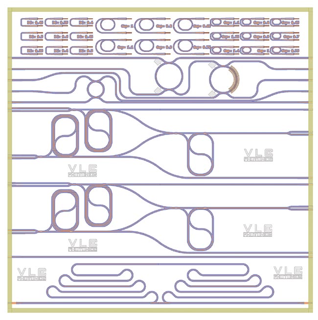
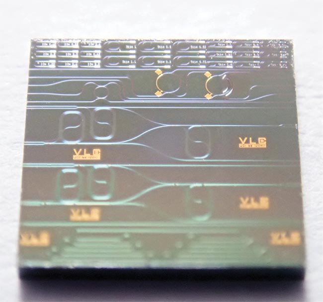
A silicon nitride (SiN) photonic integrated circuit (PIC) incorporating ring resonators and interferometers (top). PICs based on the SiN material platform are on the rise, thanks in part to the material’s comparatively better passive performance, lower prototype costs, and high performance across more wavelength ranges. The indium phosphide (InP) material platform allows direct laser integration on PICs, which makes the platform a more versatile, if comparatively expensive, choice (bottom). Courtesy of VLC Photonics.
Increased component density is a trend across the PIC industry, and it is forcing design houses and pilot lines to strike a balance between achieving absolute performance and meeting required performance. The increasing complexity is largely being driven by developments in quantum computing and automotive lidar, and there are no simple solutions for the thermal management or supply chain challenges they pose to PIC designers and their customers.
“A key trend is driving bandwidth to the edge, which, in turn, drives increasing PIC complexity at the edges of the network,” said Tim Koene, CTO at EFFECT Photonics, which is based in Eindhoven, Netherlands, and has an office in Maynard, Mass. “The performance we normally saw in core networks is now required at the edge. But we also have to deal with uncontrolled environments, which put higher demands on ruggedness and reliability, as well as a need for increased volume while costs need to come down.
PICs offer significant benefits in terms of
performance, footprint, power consumption, and bill-of-materials costs (top) compared to systems that once combined lasers and electronic components. Integrating more optical functions on chip has driven the need for larger InP wafer sizes, which have migrated from 2 in. to the 4-in. wafers in use today (bottom). EFFECT Photonics is now considering 6-in. wafers to support demand in telecom applications to help the company compete against silicon-based chips while improving performance. Courtesy of EFFECT Photonics.
“The biggest challenge, therefore, is not increasing absolute performance,” he said, “but to get the required performance, with higher requirements on ruggedness, reliability, scalability, at lower cost. In the past, PICs were mainly to drive absolute performance, and now it is to get to scalability.”
Standardization is one way to achieve scalability, but standardization is a challenge for PICs.
“Design standardization is not a problem per se, but more the standardization of the layouts towards fast and affordable testing and packaging,” said Artundo, whose company was spun off from the Universitat Politecnica de Valencia’s Telecommunications and Multimedia Applications Institute (iTEAM) and is part of the Hitachi High-Tech Group. “Some have tried to develop standard packages with their corresponding layout templates, but [the] reality is that the market applications for PICs are so varied that it is hard to come with a one-size-fits-all approach.”
Platform choices
Unlike most computer chips in electronic devices that function using electrons, PICs use photons or mixed photonic/electronic signals to transmit greater amounts of data. The most common PIC components are lasers, amplifiers, modulators, and low-loss passive elements, according to Victor Dolores-Calzadilla, an assistant professor at the Eindhoven University of Technology and a program manager for the Photonic Integration Technology
Center (PITC). Components can be integrated onto platform materials such as silicon (Si), InP, silicon on insulator (SOI), and silicon nitride (SiN). Each material platform has its own benefits and considerations.
Although SOI platforms are CMOS-compatible and more readily scalable in manufacturing, laser sources cannot be designed on the chip, which raises costs and manufacturing complexity. In contrast, InP allows direct laser integration, which makes the material more attractive, albeit more expensive, when compared to SOI1.
At Ghent University in Belgium, Abdul Rahim, the manager of ePIXfab, a nonprofit PIC-oriented alliance of academic and industrial organizations, has observed that, although silicon remains the most popular PIC platform, SiN is currently on the rise. The trend is driven by SiN’s better passive performance, lower prototyping cost, and high performance across more wavelength ranges. Rahim said multilayer platforms that combine a Si-guiding layer with one or more SiN-guiding layers are also becoming more common.
“The complexity of PICs is growing significantly in terms of density of components, especially in emerging applications,” said PITC’s Dolores-Calzadilla. One of the center’s projects, for example, aims to increase the integration density
of InP PICs and make dense optical phased arrays for high-performance beamforming.
Another example of state-of-the-art commercial PICs is a 100-Gbit/s transceiver chip designed by EFFECT Photonics. The company uses InP wafer-scale monolithic integration that incorporates lasers, modulators, photodetectors, amplifiers, and similar nonlinear elements1.
A PIXAPP laboratory in Cork, Ireland. PIXAPP is an open-access PIC assembly and packaging pilot line. Courtesy of PIXAPP.
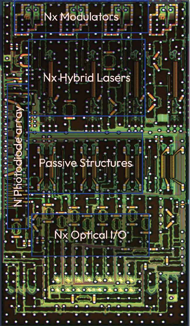
OpenLight’s 400G and 800G PIC reference designs integrate lasers, optical amplifiers, modulators, photodetectors, and other key photonic components. OpenLight introduced an open silicon photonics platform with integrated lasers designed to comply with fabrication processes at the Tower Semiconductor foundry. The technology eliminates the need to procure and align discrete lasers. Courtesy of OpenLight.
Among the companies that have developed PICs past the prototype stage, according to Rahim at ePIXfab, are iPronics in Valencia, Spain; QuiX Quantum in Enschede, Netherlands; Scantinel Photonics in Ulm, Germany; and SCINTIL Photonics in Grenoble, France, and Toronto, Canada.
Turning up the heat
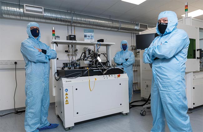
Before PICs reach the volume manufacturing stage of commercialization, they need to be prototyped, often via pilot lines. PhotonHub Europe is the central coordination point for Europe’s photonics pilot lines, including the PIXAPP Photonics Packaging Pilot Line in Cork, Ireland. Peter O’Brien, managing director of PIXAPP and head of the Photonics Packaging and Systems Integration Group at Tyndall National Institute, noted the recent increase in the density and complexity of PIC designs, which are showing larger numbers of integrated optical components and optical and electrical interconnects. As with ICs, increases in component density require improved thermal management.
“These increases have resulted in more efficient thermal management requirements and more advanced substrates or interposers for electrical routing, particularly for high-speed electrical interconnects,” O’Brien said. “This places more demands on device packaging, which can affect the overall costs of the final product.” If poorly managed, heat can affect the performance and long-term reliability of the overall module. As a consequence, PIC designers must now prepare more advanced thermal models and simulations in their work plans, he said.
Designing for thermal variability is difficult. Kevin McComber, CEO of Spark Photonics in Waltham, Mass., said it is rare for a foundry process design kit to include characterizations of materials or device performance against temperature. Although designers may know the thermal characteristics of the materials and devices available, they also need to calculate the expected temperature range of operation for each device on the PIC. This range can vary depending on the relative arrangement of active devices, such as semiconductor optical amplifiers on the chip and how the chip package distributes thermal management elements such as thermoelectric coolers.
“It can get very complicated and difficult to simulate with confidence before packaging,” McComber said. “Multi-physics simulations that take heating into
account can help overcome this, but I don’t think there is yet a silver bullet.”
A separate but no less important consideration for designers is the quality and security of their supply chain, especially if they are targeting their design for large-volume applications. “You need to take immediate steps to get to volume from day one,” said EFFECT Photonics’ Koene.
Complicating matters is the fragmented nature of the PIC supply chain. PIC designers need to monitor suppliers for potential gaps in the chain of materials and components needed for their application. “Ultimately, this will ensure they can manufacture their PIC products without unforeseen bottlenecks,” O’Brien said.
Integration and interconnection
Two methods of PIC integration making significant progress in recent years are heterogeneous and hybrid integration.
Heterogeneous integration involves processes in which InP components are either wafer-bonded over silicon wafers or grown on top of them. In contrast, hybrid integration involves gluing or soldering InP components to another PIC.
At PIXAPP, O’Brien has observed a trend toward heterogeneous integration
materials — such as InP — and co-packaging with electronics. Such co-packaging reduces the module’s energy consumption because the PIC and control electronics can share a common electrical interposer. Low-energy-consumption data centers are spurring demand for co-packaging. So is the high number of optical channels required by lidar, which O’Brien said must be designed with more efficient and closely spaced output optical couplers.
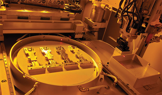
AEPONYX uses photonic wire bonding machines along with hybrid integration to develop PICs that are able to leverage many of the benefits of SiN material platforms while minimizing the material’s drawbacks. Courtesy of AEPONYX.
Heterogeneous integration is also enabling a Santa Barbara, Calif., company called OpenLight to introduce an open silicon photonics platform with integrated lasers. Using the Tower Semiconductor foundry, OpenLight has taped out its first multiproject wafer with 400G and 800G reference designs that integrate lasers,
optical amplifiers, modulators, photodetectors, and other key photonic components.
“Photonic interconnects use every means necessary to increase total data throughput. This includes speed per lane, as well as number of lanes,” said OpenLight COO Tom Mader. Currently, 800G datacom links use eight channels, he said, but he predicted that the number will increase over time to 16, 32, and 64 channels to meet the increasing requirements of cloud computing, video services, and other bandwidth-hungry applications.
“As lane counts increase, it becomes more and more difficult to combine laser sources with PIC designs,” Mader said. “[Designs do] not scale well as complexity increases. We believe that on-chip optical gain and amplification is the key to overcoming these scaling challenges for silicon photonics going forward.”
In Montréal, AEPONYX, a fabless PIC designer, is using hybrid integration methods to develop its micro-optical switches. Its SiN PIC platforms for the telecommun-
ications industry incorporate lasers, avalanche photodetectors, semiconductor optical amplifiers and modulators, and digital signal processing technology. The company has been migrating PICs into the datacom, quantum, automotive, and life science markets.
“Thanks to hybrid integration and photonic wire bonding, any perceived weakness of SiN as a platform can now be overcome for telecom, datacom, automotive, and quantum markets, while those same perceived weaknesses are irrelevant for most applications in the life science space,” said AEPONYX CEO Philippe Babin. “As for the greater photonics industry, the mass production of silicon photonics-based transceivers and InP-based, externally modulated lasers demonstrate how viable PIC-based products are.”
Babin also said advancements in photonic wire bonding have improved fabrication. During the photonic wire bonding process, a machine detects the waveguides and the facet of the components, then automatically calculates the optimal shape and dimension of the photonic wire bond. The process results in low optical losses, and the production throughput is much better than active alignment or fine placement in some cases, he said.
At PIXAPP, O’Brien said photonic wire bonding is still in research. “We have yet to see how well they can scale in manufacturing and if the polymer-based materials they use can meet long-term reliability requirements,” he said. “In my opinion, they are still at a relatively early stage of development and need to be evaluated more comprehensively before they can be considered for a manufacturing environment.”
Fabrication variability
One of the primary concerns customers have when pursuing a large-volume PIC design is the level of variability in its
fabrication process. There are ways to design for such variability, but not all
integrated photonics foundries offer
the statistical data to inform what the variability might be across many units, said Spark Photonics’ McComber.
“That makes design for manufacturing difficult.”
Dolores-Calzadilla of PITC said foundries are increasingly offering more measured data in their multiproject wafer reports. Such steps will build confidence in PIC designs and accelerate the testing and evaluation of chip performance.
Reliable statistics at both the chip and subcomponent levels are crucial to achieve high manufacturing and technological readiness levels, which are doubly important considering that a lack remains of affordable access to prototype runs before scale-up, said Nick Singh, CTO of PhotonFirst in Alkmaar, Netherlands.
In recent years, PhotonFirst has been collecting greater volumes of statistical data to help drive predictability of performance and yield for a chip design. Singh said PhotonFirst has built extensive statistical knowledge on its PIC-based fiber Bragg grating sensor systems to help manage thermal and electro-optical crosstalk, losses, and material stability.
“Predictability of yield and stability over time [are] important to assure an industrialized process,” he said.
Reference
1. A.N. Bozovich (June 16, 2020). Photonic integrated circuits (PICs) for next generation space applications. 2020 Electronics Technology Workshop (ETW), NASA Jet Propulsion Laboratory (JPL).