State-of-the-art metrology and vision systems deliver a vast amount of spatially and spectrally resolved information, requiring the optical front end to operate at higher performance than ever before.
PETER BAUER, ANDREAS BICH, AND THOMAS RUPPEL, SWISSOPTIC AG
Image sensor evolution has been extremely expansive since the first digital camera was created in 1975. In more recent years, increasing use of image sensors has rapidly driven camera chip evolution in many aspects: resolution, sensitivity, signal-to-noise ratio, speed (frame rate), and fill factor among them.
This has evolved to a point where the traditional trade-off triangle between resolution, speed, and sensitivity becomes less relevant for selection of the best components for the applications. Acquiring images with more than 100-MP resolution, capturing a few hundred frames per second, and getting readable signals under low-light conditions can be achieved today with moderate budgets.
Optical subsystem assembly. Courtesy of SwissOptic AG.
That said, the front end of the image sensor — the optics — has also adapted to the increasing performance of the imaging sensor. High-resolution sensors demand optics closer to or at diffraction limit. Increasing sensitivity opens up new application fields that require optics to be increasingly lightweight and rugged when used outdoors or in harsh industrial environments.
Additionally, the use of wavelengths outside the visible range is changing
the requirements on the optics side, including inspection in DUV (deep UV
at 193 nm), and multispectral and
hyperspectral imaging ranging from
UV to wavelengths in the IR. Essentially, modern image sensors are driving innovation on the optics side, specifically when it comes to industrial metrology. Customized optical systems are used in an increasing number of applications to provide the sensors in the optical system with enough information to really benefit from their increased performance.

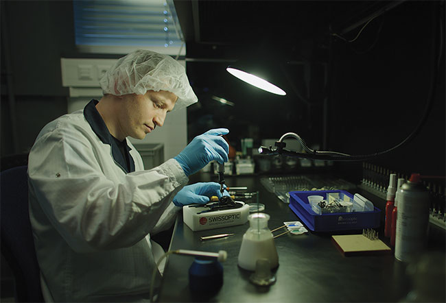
Manual cleaning prior to coating of a lens made of delicate material. Courtesy of SwissOptic AG.
Optical, mechanical designs
The design of high-end optical systems for a demanding application usually starts with the specification of the six main parameters: magnification, focal length, resolution, depth of focus, spectral range, and target customer price.
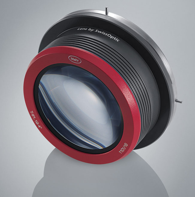
A 4-in. interferometer objective lens specifically designed to meet the needs of the innovative Tilted Wave Interferometer (MarOpto TWI 60) created by Mahr GmbH. Courtesy of SwissOptic AG.
The magnification (m, which describes the optical magnification of the physical image onto the image sensor) of an optical system should be aligned with the resolution of the image and the pixel size of the employed image sensor to make the details of interest visible. In combination with the front focal length (fo) of the optical system (given by a working distance for a specific application), the back focal length (fi, the distance from the last optical lens to the image sensor) can be calculated as fi = m × fo.
The resolution and depth of focus of
an optical system are influenced by the
f number (F#). The F# is also an important factor for image brightness (depending on the image sensor sensitivity) and is defined as F# = f/D, where f is the focal length of the optical system and D is the optical diameter. It is possible to achieve higher resolution with a larger F#, but at the same time the depth of focus (DoF) — the acceptance range for focus variations while still having a sharp image — becomes shorter. Especially in industrial metrology applications, a high DoF is desirable, as it reduces the need for refocusing. Resolution and DoF therefore need to be balanced during the design phase, whereby both benefit from bright images and good illumination conditions. As a result of diffraction, the resolution of an optical system reaches a fundamental maximum. An optical system with the ability to produce images at a resolution as good as the instrument’s theoretical limit is said to be diffraction limited.
The spectral range of the optical application describes the lowest and highest required optical wavelengths for the specific application. It strongly influences the type of glass used for optical elements (lenses, prisms, filters, etc.) and can significantly complicate the overall optical design. From a design point of view, low-dispersion glasses are most favorable for optical elements, since they require little effort to compensate for chromatic aberration but often come with short spectral ranges and high prices. As a result, the price of an optical system is strongly influenced not only by the desired resolution and magnification in the optical application, but also by the required spectral range, which drives the material cost of optical elements.
Tolerating an objective lens
Once the nominal optical design is fixed and all theoretical system parameters are achieved, the optical designer performs a so-called tolerance analysis. This procedure allows the designer to tolerate the optical elements in terms of acceptable alignment accuracies (including what is needed for mechanical mounts), as well as the manufacturing tolerances for all optical elements, such as center thickness variation, glass homogeneity, and surface irregularities. For example, demanding metrology applications such as interferometers require objective lens designs with minimal tolerances to achieve valid measurement results.
During the mechanical design phase, all alignment accuracies and application requirements are taken into account and used to build a mechanical model with classical CAD software. Here, special mounting techniques for low-stress interfaces of optical and mechanical parts are of high importance for diffraction-limited optical systems.
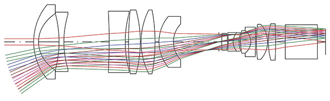
Nominal optical design of a metrology objective lens. Courtesy of SwissOptic AG.
In particular, many semiconductor applications require special gluing. Designs with large optical elements often involve special mounting strategies and flexure hinges to ensure performance in variable-temperature environments. Also, the choice of material for mechanical parts comes into play when long-term stability and large working temperature ranges are required. In some cases, mixtures of various mechanical materials with different thermal expansion coefficients are used to achieve athermal behavior. Here, choosing the right mounting technology (gluing, bonding, mechanical fixtures, etc.) requires extensive design experience and deep understanding of the customer application.
Optical element accuracy
After the mechanical design is finalized, which often includes tolerancing loops with the lead optical designer, the production of optical and mechanical parts can be started.
The required optical elements are derived from a pure block of glass, first by grinding and then by polishing the glass surface. Depending on the manufacturing process, high-precision optical elements require fine correction steps after polishing, which involves technologies such as ion beam finishing, magnetorheological finishing, or fine polishing or etching with specialized tools. However, today the accuracy of the end product is not limited by the machining tools, but by the accuracy of the metrology equipment. Surface irregularities of a few nanometers for optical elements with diameters of
50 to 500 mm are typical for optics used in semiconductor metrology applications.
In modern cleanroom metrology areas with temperature-stabilized conditions, it is possible to measure form variations below 1 nm on the entire optical surface and correct for it in a closed-loop manner. For many applications — including machine vision, medical devices, and optical microscopy — these accuracies are sufficient, but semiconductor applications always push for new limits. Even today, with modern fabrication technologies and metrology equipment, only a few companies worldwide can manufacture optical elements with high-precision requirements out of demanding glass materials. Designing and manufacturing optical systems at the edge of what is technically possible is something that requires decades of experience.
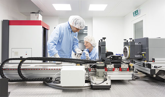
Engineers measuring surface irregularities with a large-scale interferometer. Courtesy of SwissOptic AG.
Optomechanical assembly
When all optical components are manufactured, inspected, and coated, and all mechanical parts are finished, the optomechanical assembly can be started. Ideally, the mechanical design has been performed, such that only short assembly steps are required and easy integration of tilt- and decentration-sensitive optical elements can be semi- or fully automated.
For diffraction-limited optical systems, the assembly often involves manual work and in situ metrology, using compensation strategies to achieve a perfectly aligned optical system. In many cases, specialized assembly and metrology setups must be developed to allow assembly, iterative use of metrology, and functional testing at or close to the environmental working conditions of the final application.
Lenses designed and manufactured for high-resolution and diffraction-limited performance under harsh environmental conditions require a seriously planned final quality check, as well as quality tests for its subassemblies, checking for well-centered lenses with low tolerances on tilt, decentration, center thickness, and precise interlens distances. For diffraction-limited performance, optical compensators are sometimes inevitably adjusted in the micron and even submicron range during final assembly to meet all of these requirements.
Correct treatment, neat handling, proper storage, and careful cleaning of optical and mechanical parts throughout the entire production process, especially for the DUV domain, is a must. And assembly in special cleanrooms is a necessity.
For multispectral or high-resolution applications, beamsplitter prisms come into play to create the increasing spectrum for multichip sensors or to apply superresolution technologies. Sensors should be mounted very precisely in the order of
0.3 μm and must remain stable over temperature drifts and time. This implies using a very precise measurement technology in combination with a stable assembly technology that includes special adhesives or new mounting technologies for prisms and sensors. Completing the system with electronics and image sensors according to the needs of the final applications and the demands of the respective customer is another step in generating customized optical systems. Once this is done, the assemblies are ready to be shipped and used, for example, in 3D scanners as lenses for specific machine vision applications or as measurement devices in other industrial metrology applications.
While many of today’s imaging applications can be addressed with standard optics, the general increase in image-based metrology systems in the industry is also driving the demand for diffraction-limited optical systems. With a large variety of applications increasing demands on resolution, sensitivity, and spectral range, the optics’ performance levels continue to rise. The result: new limits for surface accuracy of optical elements, mechanical design, and assembly technologies.
Higher-performing metrology systems will translate into improved productivity, increased yield, and enhanced production quality for cars, food, and smartphones.
Meet the authors
Peter Bauer is a business development manager at SwissOptic AG. He has 20 years of experience in the optics industry and in various end customer markets using light as a tool. Bauer has a master’s degree in geology from Justus Liebig University Giessen, Germany, and an executive MBA from the University of
St. Gallen, Switzerland.
Andreas Bich is head of product development for the metrology business unit at SwissOptic AG. He has 13 years of experience in metrology, manufacturing, and design of optical components and systems. He studied applied photonics at Aalen University in Germany.
Thomas Ruppel is director of technology at SwissOptic AG. He has 12 years of experience in research and development of optical systems and optical fabrication technology. He studied cybernetics at the University of Stuttgart and holds a doctoral degree in control engineering of adaptive optical systems from the University of Arizona and the University of Stuttgart.