CMOS image sensors are a critical component of the automatic optical inspection systems used in the microelectronics industry. Before being incorporated into such systems, the sensor should undergo a series of performance and cleanliness checks, down to the pixel level.
David Harel, CARMEL FORGE LTD., and Doron Nakar, NOVA LTD.
Automatic optical inspection (AOI) systems provide fast, noncontact, and reliable high-resolution defect recognition for the microelectronics industry and are widely used and incorporated into
the industry’s in-line production flow.
In-line inspection machines must be fast enough to meet or exceed the takt time of the line to avoid affecting production throughput.
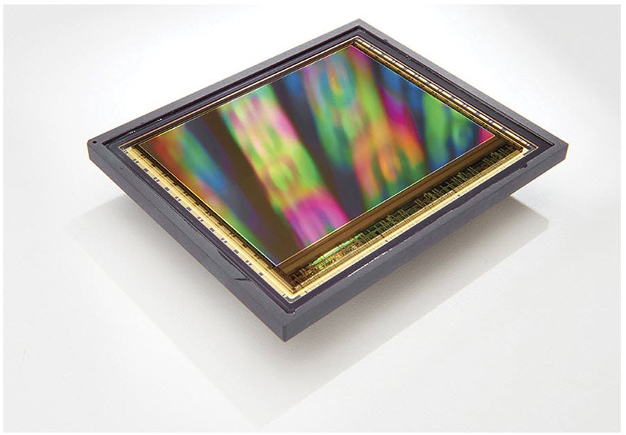
A typical CMOS sensor for automatic optical inspection (AOI) applications. Courtesy of Teledyne DALSA.
A typical AOI system includes an image sensor (either a 1D line scan or a 2D area scan), most commonly a CMOS sensor; a lens to image and magnify the scanned area onto the sensor; and light sources, such as LEDs, that illuminate the panel from the top or bottom. Other components include an image acquisition and preprocessing card and a PC for real-time image processing to detect, classify, and report defects.
The image sensor, lens, and top light source are incorporated into a single AOI camera. Often, several cameras will scan in parallel panes to increase the coverage area and reduce inspection time (Figure 1). Up to several square meters are scanned at once, which requires multiple image processing cards and computers to acquire images and process them simultaneously at high data rates. The image sensor must be capable of acquiring hundreds of frames per second. It must also be sensitive and exhibit low noise to provide high-resolution images.
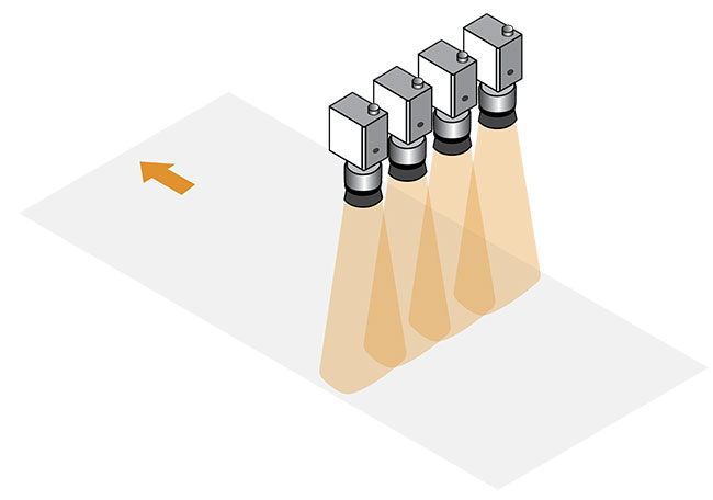
Figure 1. An AOI scanning system. Several static cameras arranged in a row scan a single panel in parallel. The scanned panel moves simultaneously with image acquisitions to cover the entire panel’s surface. Courtesy of David Harel and Doron Nakar.
A typical defect measures from one to a few microns, covering only a few pixels in the projected image on the sensor. Therefore, high-quality and sensitive pixels are crucial for defect recognition.
Inspecting CMOS sensors
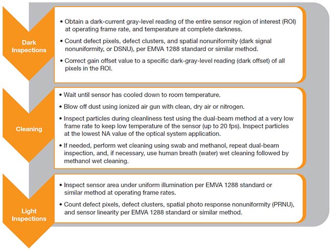
AOI defect recognition requires sensors that are completely clean. Before an CMOS image sensor or a camera is integrated into an AOI system, it usually must undergo incoming performance and cleanliness checks down to the pixel level.(See the Recommended Sequence table.)
Sensor performance tests are determined by the image sensor’s application and usually include tests performed in complete darkness as well as under uniform illumination. Such tests are described, for example, in the European Machine Vision Association (EMVA) 1288 standard for the characterization of image sensors and cameras for machine vision applications1.
Measurements taken during such tests include those of white blemish pixels and white clusters (several pixels combined together) that have gray-level readings — that is, white pixels — above a certain threshold value under complete darkness. Also, nonuniformity of the gray-level reading across the sensor’s region of interest is defined and tested under dark conditions (dark signal nonuniformity).
Gray-level readings for pixels and clusters are also obtained under complete uniform illumination to find black blemish pixels — that is, pixels with gray-level readings below a defined threshold — and even “dead” pixels. Spatial uniformity (photo response nonuniformity) and a sensor’s linearity are also tested under various illumination intensity levels.
Unlike with a sensor under dark conditions, with an illuminated sensor, if the sensor’s cover window is not perfectly clean, the pixels underneath dirt or a stain might appear darker and be mistakenly classified as blemish pixels. Therefore, it is highly recommended that a cleanliness check be performed before conducting a performance test under uniform illumination.
Dual-beam cleanliness test
In the dual-beam test, a sensor is uniformly illuminated at two different angles at different time frames, and then images are taken. By comparing
the two images and inspecting the blemish pixels’ sizes and locations, each suspected spot on the cover window can be easily classified as either dirt that can be cleaned, or as damaged pixels that could disqualify the sensor. The principle illustrated in Figure 2 is simple: The shadow caused by dirt or a particle on the cover window moves with the illumination angle by a certain distance that can easily be calculated by knowing the illumination angles’ and sensors’ geometry. On the other hand, a blemish pixel spot does not move with change of the illumination angle between the images.
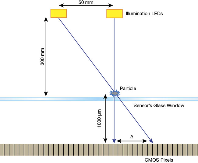
Figure 2. An illustration of the dual-beam
cleanliness test concept. A particle with a 6-µm pixel size that is located on the glass cover of the CMOS sensor partially blocks the light coming
toward the sensor. Two LEDs located 300 mm away from the sensor and 50 mm apart from each other illuminate the sensor at different time frames, and two images are taken by the sensor. The shadow of the particle moves from image to image according to the following simple geometric calculation:

A shift of the spot by 28 pixels can be easily detected and classified as ‘real dirt’ by comparing the two images. Courtesy of David Harel and Doron Nakar.
It is important to note that a sensor’s sensitivity to dirt depends not only on the particle’s size but also on the converging or diverging angle of the light. In other words, the sensor’s numerical aperture (NA) plays an important role in the sensor’s sensitivity to dirt.
As illustrated in Figure 3, the lower the sensor’s illumination NA, the higher its sensitivity to dirt, due to the partial shadow effect. In practice, in the dual-beam cleanness test, the illumination NA (of both beams) is dictated by the LED’s size and distance to the sensor and should not exceed the sensor’s
application NA of the AOI system. In other words, in the cleanness test, the illumination beams should be as collimated as possible to increase test sensitivity to particle size.
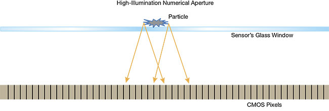
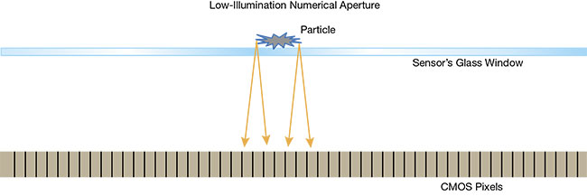
Figure 3. An illustration of the impact of the
illumination’s numerical aperture (NA) on a sensor’s sensitivity to detect dirt. High NA leads to more light coverage of the pixels underneath the particle (top), whereas at low NA, the partial shadow area is smaller, leading to more pixels with lower gray-level readings underneath the particle (bottom). Courtesy of David Harel and Doron Nakar.
Ionized air or nitrogen
The first rule for cleaning optics is: If it is not dirty, do not clean it, because damage to an optic can result from
improper cleaning attempts. The use of a cleanroom environment (Class 1000 or above) is recommended for the cleaning and assembly of an AOI
module. Optical elements such as lenses, mirrors, beamsplitters, and CMOS image sensors are usually already clean when packaged and shipped from suppliers. If a slight amount of dust appears on the surface, it can easily be blown off by using
ionized, clean, dry air or clean nitrogen.
The first rule for cleaning optics is: If it is not dirty, do not clean it, because damage to an optic can result from improper cleaning attempts.
Ionized air or nitrogen is preferred because dielectric surfaces — such as a glass window, for example — can attract particles and dust if electrostatically charged. To discharge the surface, blow ionized air onto the surface.
Wet cleaning
If sticky particles or stains remain on the surface after attempts are made to blow them off, a wet cleaning may be necessary. But before making this determination, perform a dual-beam cleanliness test, which should indicate whether a wet cleaning of the sensor’s glass surface is necessary. The favored cleaning solvent for the
wet cleaning of optics is high-purity methanol (CMOS-grade or above) because it is a more volatile solvent compared to ethanol or isopropanol. Additionally, methanol, unlike acetone, will not attack some plastics. Mixing
solvents is also common in optics cleaning. Refer to the suppliers’ technical information about solvents to avoid irreversibly damaging the sensor’s surface or peripheries.
Wet cleaning should be performed using a cleanroom-grade, nonwoven, lint-free polyester swab, such as
Texwipe swabs.
The Recommended Sequence of the Incoming Inspection of an Imaging Sensor
Users should follow safety instructions and wear safety glasses and gloves before performing a wet cleaning using methanol. Also, because
performance tests are usually conducted at an operational frame rate of hundreds of frames per second (and also in darkness), the sensor temperature could rise up to as high as 30 to
40 °C above room temperature.
Therefore, users should wait for the sensor to cool down before starting wet cleaning.
Using a push-down dispenser, soak a small amount of methanol onto a swab. Remove any excess solvent on the swab by shaking it several times. Apply gentle force on the sensor’s glass cover and move the swab in a straight line from side to side across the sensor’s active area without removing the swab from the surface in the middle of a single pass. Avoid touching the sensor’s sharp corners or edges with the swab, and start and finish the swab contact with the window on the glass surface but outside the sensor’s active area. Up to three passes for a single wet cleaning attempt is sufficient. Perform another dual-beam test afterward to check whether the cleaning was successful.
Some organic stains are not soluble using alcohol-based solvents. For such cases, a polar solvent such as water should be used. The best water-based cleaning method uses human breath, which is basically natural distilled water. For this process, generate a small film of moisture by breathing on the sensor’s surface (make sure not to drop any saliva droplets on the sensor) and immediately follow by passing a swab with gentle force. Repeat this step several times, if necessary, and always follow this process with a methanol cleaning as a final wet clean.
Meet the authors
David Harel is a product engineer at Carmel Forge Ltd. in Tirat Carmel, Israel. He was previously a lab engineer at Tel Aviv University and Technion -
Israel Institute of Technology. He
received a bachelor’s degree in
mechanical engineering and a master’s degree in system engineering, both from Technion; email: [email protected].
Doron Nakar is product lead engineer at Nova Ltd. in Rehovot, Israel. He was previously an automatic optical inspection (AOI) quality and manufac-
turing engineer at Orbotech Ltd. He
received a bachelor’s degree in
mechanical engineering and a master’s degree in electro-optics and solar
energy from Technion - Israel Institute of Technology and Ben Gurion University, respectively; email: [email protected].
Reference
1. European Machine Vision Association (EMVA) (2021). Standard 1288: Standard Characterization of Image Sensors and Cameras, Release 4.0, www.emva.org.