Defects matter when it comes to optical surfaces, but knowing what types of flaws are acceptable requires a combination of surface inspection and close communication between supplier and user.
MARIE FREEBODY, CONTRIBUTING EDITOR
It may come as a surprise to learn that, in sharp contrast to the high-precision practices of the optics industry, many optical surfaces are still inspected by the naked eye. Humans have yet to be usurped by automation, in this niche at least, but automated inspection could become an increasingly useful option if current trends continue.
Optical inspections utilize a host of techniques to reveal surface details that are difficult or impossible to be seen with the naked eye, and these techniques give rise to a wide array of specifications with equally numerous and confusing terminology. In the end, though, establishing the correct specification comes down to determining whether and how surface defects may affect the optical system and its intended use.
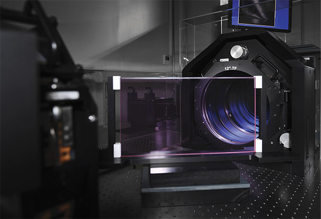
In addition to the human eye, a range of optical equipment is used for close inspection of optical surface texture, including large-aperture interferometers, white-light interferometers, and atomic force microscopes. Courtesy of SCHOTT.
In concept, optical surfaces are idealized perfect shapes, although in the real world no surface can be made without blemish. Imperfections can arise during manufacturing, when surfaces are exposed to the environment prior to packaging, or even when an optic is in transit. Any scratch, dig, chip, stain, bubble, or discoloration could compromise the performance of the optical system and affect the application for which it was designed.
Often, scratches and digs have little impact on the actual performance of an optical system but are instead indicative of the care and workmanship of the optical fabrication. The crucial factor to keep in mind is the acceptable number, type, and severity of defects. The types of imperfections that customers need to look out for vary widely depending on the application.
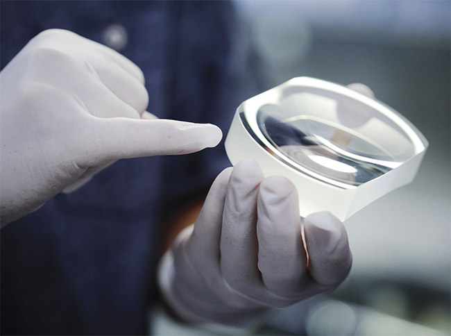
No optical surface is entirely free of defects. Imperfections can arise during manufacturing, when surfaces are exposed to the environment prior to packaging, or when an optic is in transit. Any scratch, dig, chip, stain, bubble, or discoloration could compromise the performance of the optical system and affect the application for which it was designed. Courtesy of asphericon GmbH.
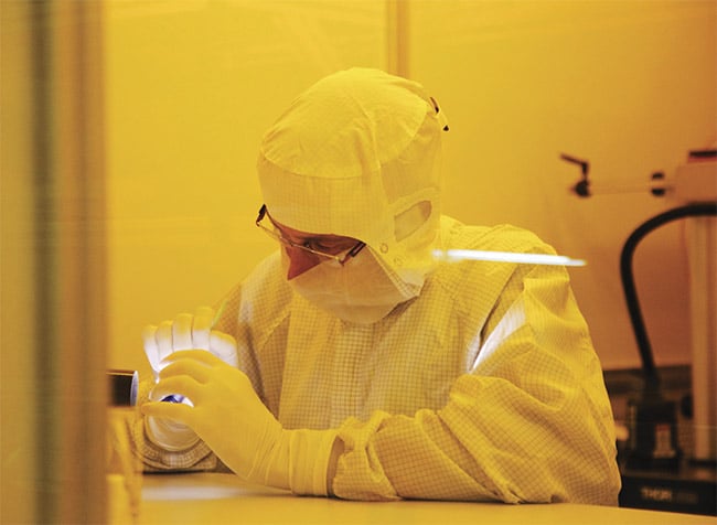
Inspecting surface quality following the MIL-PRF-13830B specification involves performing a visual inspection and comparing the surface to a calibrated standard to characterize the level of visible defects. Courtesy of asphericon GmbH.
Laser applications, for example, can have a particularly low threshold for surface flaws. “For high-power laser systems, the smallest amount of contamination could lead to laser-induced damage, reducing performance and possibly even leading to system failure,” said Cory Boone, lead technical marketing engineer at Edmund Optics. “[Low] surface roughness may also be important for minimizing scatter, as high-power laser light scattering through a system could be dangerous.”
However, in lower-power laser applications, surface roughness may have a negligible effect on performance, and maintaining a tight roughness specification will unnecessarily increase cost.
“A super-polished window with a surface roughness less than 1 angstrom may be needed for a precise, high-power laser materials processing system in order to minimize scatter, but the same window would be drastic overkill as a protective window in a low-power light projection system,” Boone said.
Scratches and digs
Since the possible permutations of type, magnitude, and number of surface defects is so vast, no single overarching standard can specify the quality of an optical surface. Over the years, however, two commonly accepted standards have emerged to try to bring clarity to the industry: the U.S. Military Performance Specification MIL-PRF-13830B and the European-originated ISO 10110.
When measuring to the MIL specification, an optic’s surface is visually compared to a calibrated standard. A 100-W fluorescent lamp is often used to enhance the visibility of any defects, while a more detailed comparison to the standard is performed using a 40-W lamp.
The MIL standard format follows a scratch number approach, followed by a dig number based on calibrated standards. Specifically, there are five scratch numbers — 10, 20, 40, 60, and 80 — where the brightness of scratches increases from the lowest number to the highest. Dig numbers apply a similar scale. Scratch numbers are an inexact measurement of scratch brightness. Rather, they provide a scale on which to subjectively compare how bright a scratch appears against the calibrated standard. For both scratches and digs, the numbers are somewhat related to the apparent geometrical width of the defect in the optical surface.
“Scratch-dig values of 40-20 are generally thought of as standard quality for many optical applications,” Boone said. “Precise laser applications usually require a scratch-dig of 20-10, and the most demanding laser applications, such as intracavity optics, typically require a scratch-dig of 10-5.”
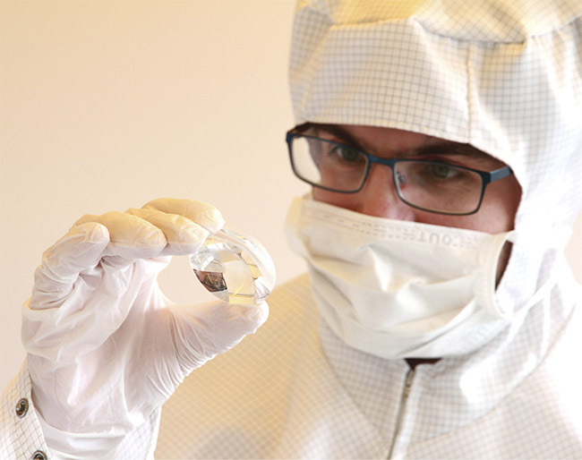
An expert eye is needed to inspect optics for surface imperfections, but the task is time-consuming and adds cost. Automated systems capable of inspecting parts according to specific standards or tailor-made specifications already exist, but they are not yet connected to deep learning. Courtesy of asphericon GmbH.
A laser’s wavelength can also influence how stringently the surface quality of its optics is toleranced. The shorter wavelengths of a UV laser, for example, will often require optics with a scratch-dig surface quality of 10-5. However, a 10-5 optic used with a CO2 laser operating in the infrared could be overkill, as well as needlessly expensive.
It is common for high-end optics to have zonal specifications to keep the costs balanced, said Ulrike Fuchs, vice president of strategy and innovation at asphericon GmbH. “Very clean” lenses are more expensive, she said, and this
cost increases significantly for larger optics.
“If measuring surface quality to the ISO specification, the number and size of surface defects is quantified,” Fuchs said. “For example, ISO 10110 5/2 × 0.025;
L2 × 0.004 translates to two defects or digs with a maximum surface area of (0.025 × 0.025) mm2 and two scratches with a width of 4 µm. This would be
suitable for most laser applications but is not the end of what is possible.”
Quality versus cost
The consensus among manufacturers
is that explicitly stipulating the quality
specifications or defect thresholds is tricky for even the most common imaging and laser applications because specifications vary tremendously depending on
the conditions of use, as well as a part’s exact function. This is where open communication between the end user and supplier becomes imperative.
Overlooking environmental demands and the influence of the other components within the system can be costly in both time and money. According to Angelo Chittani, quality manager at SCHOTT Advanced Optics, the worst results come when alignment between supplier and customer is lacking.
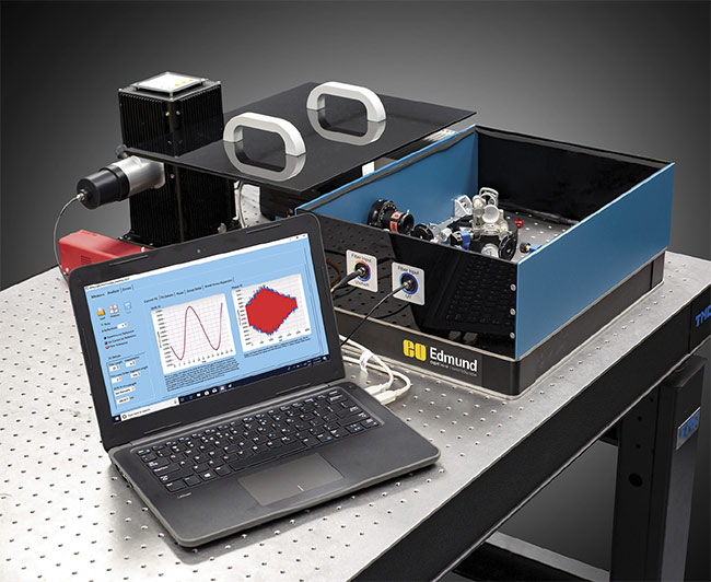
White-light interferometers are often used to measure the mid-spatial-frequency errors that contribute to surface roughness. Roughness affects scatter off of optical surfaces, which is especially important in high-precision or UV systems. Courtesy of Edmund Optics.
“It starts from understanding the customer’s need,” he said. “An offer or a specification should always talk about inspection conditions. The customers are often specialists in optical system design but have never polished or coated a piece of glass. Thus, communication and
mutual understanding are paramount.”
The founder and president of Optikos Corp., Stephen Fantone, agreed that the best results come when both parties have a good understanding of the relationship between component tolerances and system performance. He said that establishing the proper tolerance of a design is one of the most crucial steps and one that is too often overlooked.
“Designers should not rely on standard
or default tolerances,” Fantone said. “People often underestimate the time and energy it takes to properly specify and tolerance a design. I have been involved in efforts where the tolerance activity dwarfed the optical design activity. This is due, in part, to the fact that the optical system is not just lenses or mirrors, it is usually a combination of optics, electronics, and mechanics to hold it together, and optical systems are frequently used in environmentally demanding conditions.”
There are no shortcuts here, and, as Fuchs pointed out, no accurate way is available as of yet to simulate the effects that defects have in a system. For example, ISO 10110 does not specify the depth of a defect, which means it’s possible for two optical surfaces to have the same defect size but different optical behavior, depending on wavelength.
Boone advises buyers who don’t have a good feel for how certain surface roughness or surface quality translates to real-world performance to contact their optics supplier to make sure application needs are met without paying for overspecified surfaces.
The challenge of automation
An aging population across developed nations in both the West and the East, coupled with a decreasing workforce age, is driving broader adoption of automation across several industries, including the optics sector. For example, in Switzerland, SCHOTT’s Chittani cites very high labor costs as a key factor that is driving increased demand for automating optical inspection tasks — both to reduce cost and to increase the accuracy, repeatability, and reproducibility of results.
Manual surface inspection is typically carried out by experts using large-aperture interferometers, white-light interferometers, or atomic force microscopes under various illumination sources, which are determined according to a specified standard and the parts under examination.
This makes multisurface and bulk imperfection inspections highly time-
consuming. Although some automation of these inspections is possible, the technology is still too slow and can contribute significantly to manufacturing costs.
Chittani also points out that automatized inspection is limited to certain angles of incidence and that simply tilting the parts may reveal other defects that were not previously visible to the system. As a result, human inspections are more flexible and reproducible, but the judgment of human inspectors is less repeatable and remains more subjective than that of automated systems.
Savvy Optics, an optical and engineering design company with a focus on
surface inspection, offers an automated MIL testing setup, and several other companies provide various approaches for inspections according to ISO 10110. However, asphericon’s Fuchs highlights the limitations of today’s automated inspection.
“Although these inspection systems work well for small lenses such as contact lenses, scanning is soon needed when it comes to larger diameters, and systems
need to be adapted when the lenses become too steep for inspection,” she said. “Thus, automation works for limited geometries and there is still a long way
to go before this is faster than inspection by a person.”
A system that can handle any geometry up to 100 mm in diameter and that detects and classifies surface imperfections, as well as measuring the effects the defects cause, would be a game changer, according to Fuchs.
“It would make it easier to classify the surface imperfections ‘allowed’ for a certain application,” she said. “Additionally, the first testing could be carried out during manufacturing, when [components] are on their holders, as well as later on for final inspection.”
Spatial frequency range
A concept that needs broader appreciation, according to both Edmund Optics’ Boone and Optikos’ Fantone, is that every piece of metrology instrumentation measures over a certain spatial frequency range, which means that stipulating surface measurements without the associated spatial frequency qualification renders the information incomplete and sometimes useless.
“For example, large-aperture interferometers measure low-spatial-frequency errors (or figure), white-light interferometers typically measure mid-spatial-
frequency errors (or waviness), and atomic force microscopes measure high-spatial-frequency errors,” Boone said.
If all optical manufacturers called out spatial frequency bandwidths, comparisons between components and even across suppliers would be much clearer. Rather than specifying a surface roughness of “less than 2-nm rms,” for example, a fully defined specification would call out a surface roughness of “less than 2-nm rms over a 2.5- to 80-µm spatial band.”
“A lens with a large-scale and slowly varying surface deformation may be
acceptable for one particular wavelength, for example,” Fantone said. “That same peak-to-valley error at high spatial frequency will cause the surface to act as a diffraction grating. A simple statement
of acceptable peak-to-valley surface error is incomplete unless coupled with an
associated range of spatial frequencies.”
Boone recommends contacting the optical component supplier to learn how their specifications are measured. “For example, a supplier able to describe the type of metrology used and its spatial frequency range inspires more trust in
the optics meeting their advertised specifications,” he said.